


1. Introduction
Transition metal nitride coatings are being used for protection of substrates in extreme environments such as aircraft and jet engines, since they have not only high-temperature hardness, resistance to thermal and mechanical fatigue, strong adherence, chemical stability and low friction coefficient but also excellent hardness or durability.1-4) Among them, NbN coatings have excellent hardness or durability and are produced by diversified coating methods owing to such characteristics. Recently, not only dc (direct current) sputtering but also coating equipment such as hybrid sputtering and ion plating are being utilized.5-7) In particular, the dc sputtering method is widely used due to advantages of having broad application range for being capable of providing not only excellent reproducibility and adhesion but also high deposition rate and coating of complicated compositions at low substrate temperatures. However, it has disadvantages of being unfavorable in property aspects as the microstructure shows irregular columnar structures with generation of porous coatings.8) Therefore, in the present study, attention has been directed to the asymmetric bipolar pulse sputtering method which can control characteristics of coatings by providing variations in duty cycle applied to the target as an important variable for pulse plasma and in application method of pulse frequency. Particularly, since the asymmetric bipolar pulse sputtering method employs pulse power supply as compared with the existing dc sputtering method, arc production is basically suppressed due to the existence of time for application of (+) voltage. Thus, defects in the specimen produced by fine arcs can be prevented accompanied by enhancement in plasma stability. Also, as the asymmetric bipolar pulse sputtering method is reported to have higher ion flux and wider ion energy distribution in comparison with the dc sputtering method, the increase in ion flux having high ion energy is considered to have large effects on composition, texture coefficient, microstructure, and properties, etc. of the coatings.9) The studies reported thus far on NbN coatings are primarily on the use of dc sputtering method, most of which involve variations in the amount of flown-in nitrogen, the substrate temperature and the deposition time as coating process variables.10-12) In particular, no study results of quantitative analysis and consideration have been reported for the effects of plasma process variables such as duty cycle and pulse frequency using the asymmetric bipolar pulse sputtering method on crystal structure, surface and cross section microstructure, grain size, etc. of the NbN coatings.
Consequently, in the present study, NbN coatings were produced under the total of 4 types of asymmetric bipolar pulse sputtering conditions to investigate the effects of pulse plasma process variables on the properties of NbN coatings. Here, attention was directed to the effects of pulse plasma variables on microstructural changes such as nano grain size, 2-dimensional surface and cross section observations, 3-dimensional morphology and surface roughness for consideration. In addition, the effects on mechanical-physical characteristics such as preferred orientation, residual stress and nano-indentation hardness were considered.
2. Experimental Procedure
In the present experiment, 4 types of NbN coatings were produced as shown in Table 1 by using the asymmetric bipolar pulse sputtering where pulse plasma process variables could be controlled. As the starting raw materials, Nb target of 3″ in diameter, 1/4″ in thickness and 99.9% in purity, Ar and N2 gases of ultrahigh purity were used. Injected amounts of Ar and N2 were fixed at 20 sccm and 10 sccm, respectively. The distance between the substrate and the target upon deposition was maintained at 60 mm, and the substrate was rotated at a speed of about10 rpm for uniform coating. To remove impurities on Si (100) substrate surface, the substrate as washed for 10 minutes each in acetone and ethyl alcohol by using an ultrasonic cleaner, followed by drying. For the initial pressure of chamber, the chamber was exhausted down to about 1.4 × 10⁻⁴ Pa by using a rotary pump and a turbo-molecular pump, while the total process pressure (Ar+N2) was maintained at 0.3 Pa. Also, to remove impurities adsorbed onto the surfaces of target and substrate, Ar plasma was generated for pretreatment for 10 minutes, respectively. To analyze crystal structure, preferred orientation and residual stress, etc. of the NbN coatings obtained, high-resolution XRD (PAN Analytical Company / X’pert- pro MRD) was employed, while microstructures of surface and cross section of the coatings were observed by using FE-SEM (Hitachi Company/ S-3500N). To measure 3-dimensional morphology and surface roughness, Auto Probe Atomic Force Microscopy (AFM) (Digital Instruments Company / Nanoscope a) was employed. For measurement of hardness and elastic modulus, a nano indenter (MTS System Company / MTS XP) was used as a precision hardness tester. Hardness was obtained as a mean value through 16 times of experiments by using Berkovich diamond indenter. For measurement interval of the nano indenter, more than 10 μm was maintained so as not to be affected by the hardness measurement tip which is already executed.
3. Results and Discussion
3.1. Crystal structure and residual stress
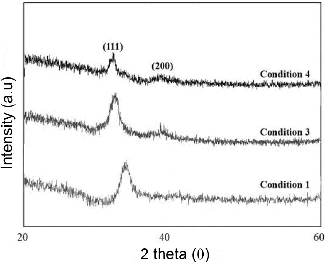
X-ray diffraction analysis results for the NbN coatings produced by the asymmetric bipolar pulse sputtering are shown in Fig. 1. Although a single phase of face-centered cubic (FCC) NbN crystal phase was affirmed for all 4 types of coating conditions, peaks of only (111) face or both (111) face and (200) face were observed depending upon the coating conditions. For example, while only (111) face was observed under the condition 1 (dc mode), peaks of (200) face, albeit weak, were also observed together with (111) face under the conditions 3 and 4 (pulse mode). In such way, multiple X-ray diffraction peaks of (111) face and (200) face were displayed under the asymmetric bipolar pulse sputtering conditions. However, no noteworthy changes in the preferred orientation of crystal faces were discovered for all coatings obtained.
Meanwhile, to investigate changes in the residual stress produced in NbN coatings as a function of coating conditions, 2θ analysis results for X-ray diffraction peaks of (111) face were examined, with the results shown in Table 2. Particularly, the standard 2θ values for NbN (111) face obtained from JCPDS card (#38-1155) are shown together to facilitate comparison of the position changes in NbN diffraction peaks as a function of coating conditions. In the case of (111) face, 2θ values for the peak were 36.87° under the condition 1, 36.87° under the condition 2, 35.67° under the condition 3, condition 4 and 35.58° under the condition 4, which can be seen to be larger than the standard value of 35.37° in the JCPDS card. In particular, the peak 2θ value for X-ray diffraction peak of (111) face can be seen to be consecutively reduced in the order of condition 1 to 4 as a function of coating conditions. Namely, such shift in 2θ values to a lower angle is reported to originate from an increase in internal compressive stress of residual stress within the coated film.13)
As the wear resistance and the hardness are increased since a considerable magnitude of compressive stress is generally generated in the coatings produced by using a PVD process, such compressive stress remaining in the coatings is closely related to the point defects produced by Ar+ ion bombardment.14) While increased substrate temperature, generation of highly ionized plasma species or ion bombardment effects are required to produce coatings with a dense microstructure not having a porous columnar structure, residual compressive stress of a considerable magnitude is considered to have been generated inside the NbN coating film due to the corresponding ion bombardment effects since the substrate bias voltage of −50 V was applied to the coating in the present study.15)
3.2. Microstructure
Microstructures of NbN coatings produced by the asymmetric bipolar pulse sputtering were observed by using FE-SEM, with the surface and the cross section pictures shown in Fig. 2. In the surface picture of NbN coating produced under the condition 1, an appearance of being filled with grains having a shape of pyramid-shaped tetrahedron was observed, while an appearance of being filled with very small and round-shaped grains was observed in the surface of NbN coating produced under the condition 4. Meanwhile, in the cross section picture of coating produced under the condition 1, particles and grain boundaries of a columnar structure were observed which were extended from the pyramid-shaped particles of tetrahedron observed in the surface. On the other hand, in the cross section picture of coating produced under the condition 4, a very dense cross section structure was observed to the extent where particles and grain boundaries could not be distinguished. Such densification of the coating microstructures is considered to have been obtained by production of the highly ionized plasma species resulting from generation of the pulse plasma and by an increase in nuclei generation density resulting from an increased ion current.16)
3.3. Grain size
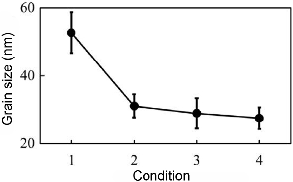
Average grain size of coatings is a very important element which controls the properties in application areas of almost all fields, and reduction in the grain size improves adhesion strength and wear resistance of the coatings by increasing the residual stress and the hardness. Therefore, the grain size and accurate measurement thereof are very important elements for optimizing application of the coatings. When a transmission electron microscope is employed for measurement of grain sizes, much time and cost are generally required for specimen production and observation. Hence, a new approach improving and simplifying this is the measurement of grain sizes by using X-ray diffraction analysis. 17) Shown in Fig. 3 is the change in grain size of NbN coatings produced by the asymmetric bipolar pulse sputtering method. While the grain size of coatings can also be calculated by the magnitude of half width of X-ray diffraction analysis peaks, the grain size is generally reduced, the larger the magnitude of half width. In the present experiment, the grain size was calculated by using the Scherrer method, and the grain size was reduced with an increase in the half width.18) As can be seen from the figure, the grain size of NbN coatings can be seen to be consecutively reduced from 52.7 nm under the condition 1, to 31.4 nm under the condition 2, to 28.7 nm under the condition 3, and then to 27.5 nm under the condition 4. Consequently, generation conditions for the pulse plasma resulting from the use of asymmetric bipolar pulse sputtering can be seen to be a very important process variable as a technique to control the microstructures of NbN coatings.19)
3.4. Morphology and surface roughness
To observe morphology and surface roughness of NbN coatings produced by the asymmetric bipolar pulse sputtering method, non-contact AFM analysis was conducted, with the results shown in Fig. 4. Considering the morphology as a function of coating conditions, surface irregularities of NbN coating produced under the condition 4 can be seen first to be reduced for smoothening in comparison with the coating produced under the condition 1. Considering the actual results of surface roughness (Ra, average roughness) as a function of coating conditions, the surface roughness of NbN coatings was reduced by the maximum of nearly 50% from 6.1 nm under the condition 1, to 5.4 nm under the condition 2, to 4.1 nm under the condition 3, and then to 3.4 nm under the condition 4. Such change in the morphology of coatings is reported to be closely related to the ion current density, and the ion current higher by about 40 ~ 80 % compared with that for dc sputtering has been reported when the pulse sputtering is actually used.20)
3.5. Nano hardness and elastic modulus
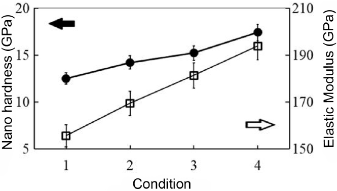
To measure hardness and elastic modulus of NbN coatings produced by the asymmetric bipolar pulse sputtering method, a nano-indentation equipment was used, and the mean values obtained by measuring at more than 30 places by the unit of 1 micrometer per sample to minimize measurement errors are shown in Fig. 5. Not only hardness measurement for the coatings with a thickness less than a few micrometers is impossible by the existing micro Vickers hardness tester but also precise measurements are very difficult due to the indentation size effects. Therefore, in the present study, measurement position of the indenter was averaged to be 1/10 spot of the total film thickness to exclude the indentation size effects which show a tendency toward an increase in the measured hardness value, the shallower the indentation depth for nano-indentation hardness measurements.21-22) As a function of asymmetric bipolar pulse plasma coating conditions, nano-indentation hardness and elastic modulus of NbN coatings can be affirmed to be increased in the order of the condition 1 to the condition 4. Namely, nano-indentation hardness and elastic modulus of the NbN coatings produced under the condition 4 were about 17.4 GPa and 193.9 GPa, respectively, showing an increase by about 30% for hardness and by up to 20% for elastic modulus, as compared with about 12.5 GPa and 155.5 GPa, respectively, for the coatings produced under the condition 1. Such increase in mechanical hardness and elastic modulus for the NbN coatings obtained by the asymmetric bipolar pulse sputtering is considered to originate from the composite elements such as high ionization of charged particles resulting from generation of pulse plasma, high Ar+ ion bombardment effect resulting from application of substrate bias voltage, grain refinement in coatings due to continuous collision of neutral atoms and molecules, and an increase in residual compressive stress, etc.
4. Conclusions
In the present study, NbN coatings were produced under 4 types of different coating conditions by using the asymmetric bipolar pulse sputtering, and an investigation was conducted for crystal structure changes such as crystal phase, preferred orientation, and residual stress of coatings, microstructural changes such as microstructures of surface and cross section, morphology, and grain size, and mechanical-physical property changes such as hardness and elastic modulus as a function of coating conditions. In all coatings, the single-phase NbN crystal phase of face-centered cubic structure was affirmed, and the peaks of (111) face or (200) face were observed as a function of coating conditions. In the surface of the NbN coating produced under the condition 4, very fine grains were observed in comparison with the coating produced under the condition 1, while a very dense microstructure was observed in the cross section. Residual compressive stress in the NbN coatings was increased in the order of the condition 1 to the condition 4, while the surface roughness was reduced so that the coating with a flat morphology was obtained. Also, hardness and elastic modulus of the NbN coating produced under the condition 4 were 17.4 GPa and 193.9 GPa, respectively, representing an increase by about 20~30 %, respectively, as compared with the coating produced under the condition 1.