Characterization of in-situ Synthesized CdSxSe1−x Ternary Alloy Nanowire Photosensor
Article information

Abstract
CdSxSe1−x ternary alloy nanowires (x = 0, 0.5, 1.0) were fabricated by in-situ synthesis on interdigitated electrode. Morphology analysis of the alloy nanowires according to the synthesis zone and composition analysis of the nanowires were carried out by SEM and EDX. The crystal structures of the alloy nanowires were studied by XRD analysis. The I–V characteristics of the nanowire photosensors were analyzed according to the intensity of incident light. The influence of zonal synthesis position on the photosensor response to the wavelength of incident light was also analyzed, and was found to be related to the bandgap of alloy nanowires. The analysis results indicate that photosensors with a specific photoresponse could be selected based on the composition of the source materials of nanowires as well as by controlling the in-situ synthesis zone.
1. Introduction
Wide-bandgap II–VI materials, such as CdTe, ZnTe, CdSe, ZnSe, and CdS have been typically used for visible light detection. Among the semiconductors, CdS and CdSe are the most promising materials for detecting visible radiation due to their primary band gap of 2.4 eV (516 nm) and 1.7 eV (729 nm), respectively, and high sensitivity.1–7) Quantitative measurement of the electron and hole mobility-lifetime products of CdS and CdSe nanowires using scanning photocurrent microscopy has provided experimental evidence that the carrier lifetime is increased in nanowires compared to that in the bulk material.8,9) Taking advantage of the photo-response properties of CdS and CdSe nanowires, photoconductors have been fabricated as ohmic contact-based devices, using techniques like dispensed nanowire suspension and e-beam lithography. Generally, nanowire photoconductors are fabricated by horizontally dispersing single nanowires or placing a nanowire mesh (either randomly distributed or aligned along a preferential direction) on an insulating substrate, and then applying an external bias between metal electrodes. Upon illumination, the electrical conductivity increases and thus provides light-sensing abilities.10–14) Nanowire photosensors have also been fabricated by dispensing and drying nanowire suspensions on interdigitated electrodes (IDEs).
In this work, synthesis of CdSxSe1−x ternary alloy nanowires was performed on the Au surface of IDE.15–18) Such a direct synthesis process of nanowires is referred to as in-situ synthesis, and the optical properties of the photosensors were analyzed according to the wavelength of the incident light and the synthesis zones in the vacuum tube.
2. Experimental Procedure
2.1. In-situ nanowire synthesis by pulsed-laser deposition
CdSxSe1−x ternary alloy nanowires were synthesized using a pulsed-laser deposition (PLD) system with a KrF excimer laser (Compex-205, Lambda Physik, Germany) excited at 248 nm. As the source material, CdS and CdSe powder was sintered at 600°C for 1 h in a hot-wall furnace (Ajeon, South Korea). The sintered target was located at the center of a quartz tube with a diameter of 5 cm in the hot-wall furnace, as shown in Fig. 1. Once the temperature reached 650°C within 15 min, the KrF excimer laser was focused on the CdS target and the laser energy density was maintained at 120–126 mJ/cm2. The synthesis temperature was maintained at 650°C for 30 min under an Ar and H2 (5%) atmosphere with a constant inner pressure of ~ 667 Pa (~ 5 Torr). IDEs with a width of 5 μm were located 9–12 cm from the sintered CdS target in the furnace tube.17–19)

Set-up for the in-situ synthesis of CdSxSe1−x ternary alloy nanowires by pulsed-laser deposition (PLD).
2.2. Photosensor measurement
The IDE was fabricated on a glass substrate using a UV-photolithography process.20,21) For the fabrication of the IDE, a positive photoresist (AZ-GXR-601) was spin-coated with a thickness of 2 μm on a 4-inch quartz wafer. After soft-baking at 100°C for 1 min, the UV-photolithography process was carried out using a photo mask for the IDE. The IDE was designed with 100 pairs of finger electrodes each with a width of 5 μm, with a space of 5 μm between the electrodes. The IDE was then baked at 180°C for 1 min. After developing the IDE pattern, a Ti layer was deposited as an adhesive layer with a thickness of 10 nm, and a layer of gold was deposited with a thickness of 100 nm by using a thermal evaporator. The IDE pattern was obtained after a liftoff process.
The photocurrent was measured using a commercial potentiostat (Compactstat) and a light-control module (IVIUM Co., Netherlands), as previously reported.19) The I–V curve from each photosensor was measured with an applied voltage range from −1.0 to +1.0 V under UV light illumination in a power range of 28.07–138.7 μW/cm2. The intensity of the incident light was calibrated using an optical power meter (New Port Co., USA). The photo-response of each photosensor was measured at an applied potential of 100 mV for various photo-intensities. The photocurrent was measured according to changes in the wavelength of the incident light by using a fluorescence spectrometer (LS-55, Perkin-Elmer Co., USA), connected to the external wave-guide cable as a light source.
3. Results and Discussion
3.1. In-situ synthesis of CdSxSe1−x ternary alloy nanowires
In-situ synthesis of CdSxSe1−x ternary alloy nanowires was carried out using PLD.15,17,19) For the in-situ synthesis of nanowires, a sintered target of nanowire material and electrodes for nanowire photosensor were positioned in the vacuum tube shown in Fig. 1. The target for PLD was sintered by mixing CdS and CdSe according to the composition of alloy nanowires. In this work, the properties of the alloy nanowires were controlled by varying the distance from the target and photosensor electrodes, and the zones for synthesis were set to be zone 1, zone 2, zone 3, and zone 4 according to the distance from the target of 9, 10, 11, and 12 cm, respectively. At each zone, eight electrodes were located for the in-situ synthesis of alloy nanowires at the same time. For the fabrication of photosensor, the interdigitated electrode was made of Au thin film with a thickness of 100 nm, which composed of 75 pairs of finger electrodes with a distance of 5 μm between the electrodes.
The morphology of the synthesized CdSxSe1−x ternary alloy nanowires was analyzed by SEM. As shown in Fig. 2, three kinds of CdSxSe1−x ternary alloy nanowires (x = 0, 0.5, 1.0) were synthesized on the finger electrodes by in-situ synthesis method. From the morphological analysis, the three kinds of CdSxSe1−x ternary alloy nanowires were observed to have more nanowire-type structures than belt-type structures according to the increase of distance from the sintered target in the synthesis tube. For CdS, nanowire composition was observed to be dominant for zone 2, zone 3, and zone 4. In the case of CdS0.5Se0.5, zone 3 and zone 4 showed a dominant composition of nanowires in comparison with other nanostructures. In the case of CdSe deposition, nearly no nanowire-type nanostructure was observed and the electrode was observed to be covered by crystal and thin film structures. EDX analysis of the three kinds of CdSxSe1−x ternary alloy nanowires (x = 0, 0.5, 1.0) showed that each alloy nanowire was composed of the source materials of each sintered target, as shown in Fig. 3. The three kinds of CdSxSe1−x ternary alloy nanowires (x = 0, 0.5, 1.0) were calculated to have the weight composition of Cd : S = 47.4 : 12.8 for CdS, Cd : S : Se = 25.6 : 2.1 : 8.9 for CdS0.5Se0.5, and Cd : Se = 41.9 : 21.2 for CdSe. The molar compositions for the alloy nanowires were calculated to be Cd : S = 0.42 : 0.40 for CdS, Cd : S : Se = 0.23 : 0.07 : 0.11 for CdS0.5Se0.5, and Cd : Se = 0.37 : 0.27 for CdSe. XRD analysis of the three kinds of CdSxSe1−x ternary alloy nanowires (x = 0, 0.5, 1.0) showed that each alloy nanowire was synthesized according to the composition of the source materials, as shown in Fig. 4. As previously reported,15,16) the XRD pattern confirmed the crystallinity of CdSxSe1−x nanowires. The single hexagonal phase was confirmed and there were no other kinds of second phases in the whole range of the composition. XRD analysis indicated that the solid-synthesized CdSxSe1−x nanowires are a solid solution. Shift in the peak position corresponding to the hexagonal phase toward a higher angle with increasing x content was also observed because the unit cell volume linearly decreased with increasing sulfur concentration. These results indicated that the in-situ synthesized CdSxSe1−x nanowires had good single crystallinity compared with the bulk and thin films reported in earlier studies.22–24)
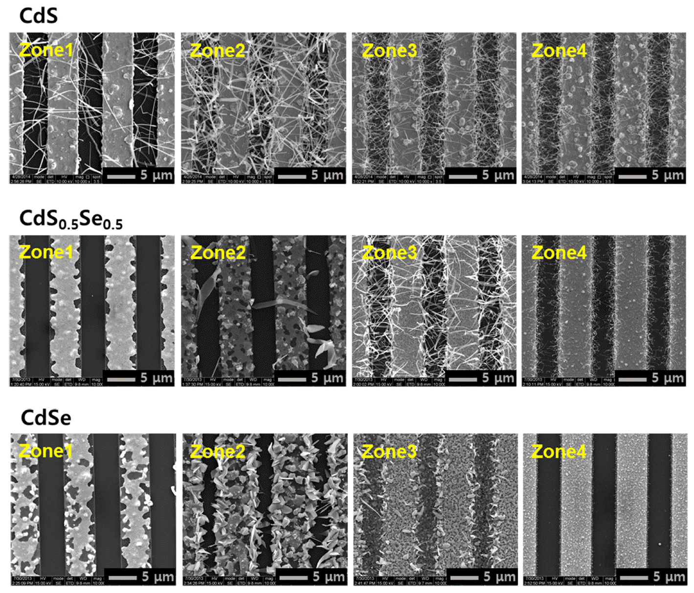
Characterization of in-situ synthesized CdSxSe1−x ternary alloy nanowires. SEM images of CdSxSe1−x ternary alloy nanowires (x = 0, 0.5, 1.0).

EDS analysis of in-situ synthesized CdSxSe1−x ternary alloy nanowires.
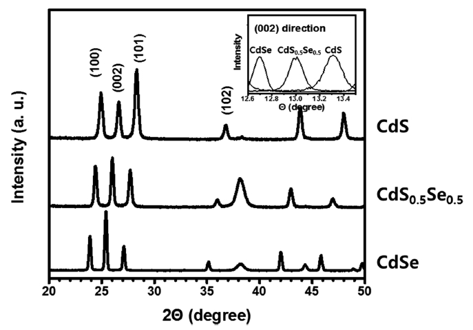
XRD analysis of in-situ synthesized CdSxSe1−x ternary alloy nanowires.
3.2. Optical properties of CdSxSe1−x ternary alloy nanowire photosensors
The nanowire photosensor was prepared by in-situ synthesis of three kinds of CdSxSe1−x ternary alloy nanowires on interdigitated electrode. The properties of the nanowire photosensors were characterized in terms of responses to the intensity and the wavelength of incident light according to the synthesis zones. Such properties were reported to be related to the contact between nanostructure and electrode surface and the electronic features of nanostructures, such as bandgaps.
As the first step, the properties of nanowire photosensors were characterized in terms of responses to the intensity of incident light according to the synthesis zones. As shown in Fig. 5, the photocurrent was measured when the input potential was applied in the range of +1.0 V to −1.0 V. The intensity of incident light was controlled to be 28.07 (μW/cm2) at the wavelength of 502 nm. The I–V response of each photosensor was measured by alternate turn-on and turnoff of the incident light. The measurement was carried out for photosensors based on three kinds of CdSxSe1−x ternary alloy nanowires according to the synthesis zones. For the photosensors of CdS nanowires, the changes in photocurrent, that is relative photoresponse, between turn-on and turn-off condition were estimated to be 4000, 4300, 11000, and 80 folds for zone 1, zone 2, zone 3, and zone 4, respectively. These results showed that the photosensors from zone 3 have the highest relative photoresponse under turn-on and turn-off conditions. In the case of the photosensors of CdS0.5Se0.5 nanowires, the changes in photocurrent between turn-on and turn-off condition were estimated to be 13, 127, and 98 folds from zone 2, zone 3, and zone 4, respectively. These results showed that the photosensors from zone 3 have the highest relative photoresponse under turn-on and turn-off conditions. In the case of the photosensors of CdSe nanowires, the changes in photocurrent between turn-on and turn-off condition were estimated to be 3.7, and 73, 30 folds from zone 1, zone 2, and zone 3, respectively. These results showed that the photosensors from zone 2 have the highest relative photoresponse under turn-on and turn-off conditions. For the nanowires including CdS, the photoresponse at turn-on and turn-off conditions was observed to be higher as the composition of nanowires was increased. Therefore, the photoresponse at turn-on and turn-off condition were determined according to the alloy composition of CdSxSe1−x nanowires as well as the type of nanostructures according to the synthesis zones.

Photoresponse analysis of in-situ synthesized CdSxSe1−x ternary alloy nanowires. I-V curves for photosensors of (a) CdS nanowires, (b) CdS0.5Se0.5 nanowires, and (c) CdSe nanowires.
As the next step, the properties of nanowire photosensors were characterized in terms of responses to the wavelength of incident light according to the synthesis zones. As shown in Fig. 6, the photoresponse of three kinds of CdSxSe1−x ternary alloy nanowires (x = 0, 0.5, 1.0) according to the wavelength of incident light was estimated. The wavelength of incident light was controlled in the range of 300 nm to 800 nm and the photocurrent change was measured continuously. The photoresponse was obtained for the photosensors of three kinds of CdSxSe1−x ternary alloy nanowires (x = 0, 0.5, 1.0), which were prepared at synthesis zone 2. The photoresponse showed that the three kinds of photosensors had a cut-off wavelength at which the photocurrent was reduced to the baseline level. For the photosensors of the three kinds of alloy nanowires of CdS, CdS0.5Se0.5, and CdSe, the cut-off wavelength was estimated to be 510 nm (2.43 eV), 620 nm (1.99 eV), and 710 nm (1.74 eV), respectively. Below the cutoff wavelength, the photoresponse was nearly at the saturated level. As reported in previous studies, the band gap of CdSxSe1−x films becomes larger with increasing x, varying from 1.74 eV (CdSe) to 2.45 eV (CdS), corresponding to the highest intensity of the samples, which matches well with our results.25–28) Thus, the photoresponse of the three kinds of alloy nanowires of CdS, CdS0.5Se0.5, and CdSe is shown to be determined by the bandgap of nanowires, which could be engineered by controlling the mixing ratio of the source materials of the sintered target.15,16)
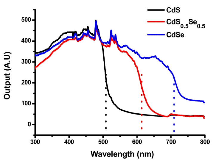
Photoresponse analysis of in-situ synthesized CdSxSe1−x ternary alloy nanowires according to the wavelength of incident light for CdS, CdS0.5Se0.5 and CdSe nanowires.
The I–V curves for the photosensors of CdSxSe1−x ternary alloy nanowires (x = 0, 0.5, 1.0) at different synthesis zones were estimated with the intensity of incident light in the range of 7.9–33.4 (μW/cm2) for the wavelength of 415 nm, 28.07–138.7 (μW/cm2) for the wavelength of 502 nm and 8.8–66.4 (μW/cm2) for the wavelength of 620 nm. As shown in Fig. 7(a), the photosensor of CdS nanowires was observed to have significantly higher photoresponse at the wavelength of 415 and 502 nm in comparison with that at 620 nm. Such response was also observed for the CdS photosensor from synthesis zone 1, zone 2, and zone 3, as shown in Fig. 7(a)–(c). In the case of zone 4, the absolute value of photoresponse was far lower than those from the other synthesis zones, as shown in Fig. 7(d). As shown in Fig. 8(a)–(c), the photosensor of CdS0.5Se0.5 nanowires was observed to have significantly higher photoresponse for synthesis zone 3 at the wavelength of 415 and 502 nm in comparison with the photosensors from synthesis zone 2 and zone 4. The photoresponse of synthesis zone 3 was estimated to be in the micro-ampere range, which was far higher than the nano-ampere range photoresponse for the other synthesis zones. The photosensor of CdS0.5Se0.5 nanowires was observed to have significantly higher photoresponse at the wavelength of 415 and 502 nm in comparison with that at 620 nm. As shown in Fig. 9(a)–(c), the photosensor of CdSe nanowires was observed to have significantly higher photoresponse for synthesis zone 2 at the wavelength of 415 and 502 nm in comparison with the photosensors from synthesis zone 1 and zone 3. The photoresponse of synthesis zone 2 was estimated to be in the micro-ampere range, which was far higher than the nano-ampere range photoresponse for the other synthesis zones. The photosensor of CdSe nanowires was observed to have significantly higher photoresponse at the wavelength of 415 and 502 nm in comparison with that at 620 nm. These results showed that the photoresponse of the in-situ photosensor was determined by the alloy materials and the synthesis zones. In other words, photosensors with a specific photoresponse for the intensity and wavelength of the incident light could be selected by controlling the synthesis zones.
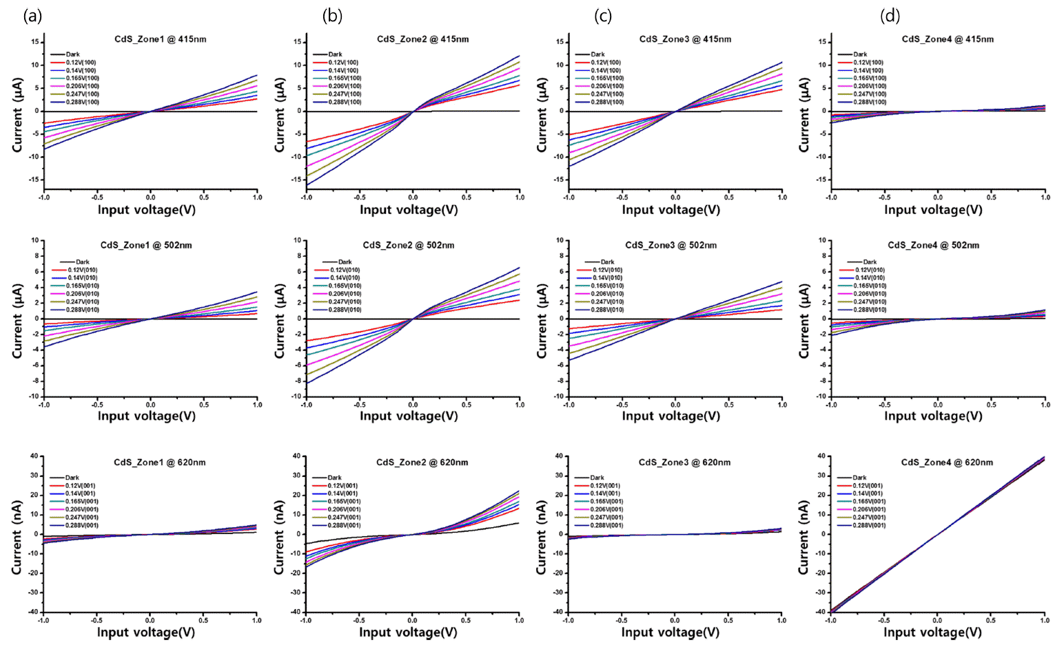
Photoresponse of in-situ synthesized CdS nanowires according to the wavelength of incident light at (a) synthesis zone 1, (b) synthesis zone 2, (c) synthesis zone 3, and (d) synthesis zone 4.

Photoresponse of in-situ synthesized CdS0.5Se0.5 nanowires according to the wavelength of incident light at (a) synthesis zone 2, (b) synthesis zone 3, and (c) synthesis zone 4.

Photoresponse of in-situ synthesized CdSe nanowires according to the wavelength of incident light at (a) synthesis zone 1, (b) synthesis zone 2, and (c) synthesis zone 3.
4. Conclusions
In-situ synthesis of CdSxSe1−x ternary alloy nanowires was carried out using PLD. From the morphological analysis by SEM, three kinds of CdSxSe1−x ternary alloy nanowires were observed to have more nanowire-type structures than belt-type structures according to the increase of distance from the sintered target in the synthesis tube. EDX analysis of the three kinds of CdSxSe1−x ternary alloy nanowires (x = 0, 0.5, 1.0) showed that each alloy nanowire was composed of source materials of each sintered target. The XRD pattern confirmed the crystallinity of CdSxSe1−x nanowires. Existence of the single hexagonal phase was confirmed and there were no other kinds of second phases in the whole range of the composition. The properties of nanowire photosensors were characterized in terms of responses to the intensity and the wavelength of incident light according to the synthesis zones. Such properties were reported to be related to the contact between nanostructure and electrode surface and the electronic features of nanostructures, such as bandgaps. From I–V analysis of the photosensors of CdSxSe1−x ternary alloy nanowires (x = 0, 0.5, 1.0) at different synthesis zones, it was observed that the photoresponse of in-situ photosensors was determined by the alloy materials and the synthesis zones. In other words, photosensors with a specific photoresponse for the intensity and wavelength of the incident light could be selected by controlling the synthesis zones.
Acknowledgments
This work was supported by the Nano-Convergence Foundation [grant number: R201602210] funded by the Ministry of Science, ICT and Future Planning (MSIP, Korea) and Ministry of Trade, Industry and Energy (MOTIE, Korea) and the National Research Foundation of Korea [grant numbers: NRF-2017R1A2B4004077].