Effective Oxygen-Defect Passivation in ZnO Thin Films Prepared by Atomic Layer Deposition Using Hydrogen Peroxide
Article information

Abstract
The intrinsic oxygen-vacancy defects in ZnO have prevented the preparation of p-type ZnO with high carrier concentration. Therefore, in this work, the effect of the concentration of H2O2 (used as an oxygen source) on the oxygen-vacancy concentration in ZnO prepared by atomic layer deposition was investigated. The results indicated that the oxygen-vacancy concentration in the ZnO film decreased by the oxygen-rich growth conditions when using H2O2 as the oxygen precursor instead of a conventional oxygen source such as H2O. The suppression of oxygen vacancies decreased the carrier concentration and increased the resistivity. Moreover, the growth orientation changed to the (002) plane, from the combined (100) and (002) planes, with the increase in H2O2 concentration. The passivation of oxygen-vacancy defects in ZnO can contribute to the preparation of p-type ZnO.
1. Introduction
Zinc oxide (ZnO) is a semiconductor material with a direct bandgap energy of 3.37 eV and exciton binding energy of 60 meV. ZnO has attracted remarkable attention owing to its outstanding optoelectronic properties and wide application scope1–4) including light-emitting diode (LED) displays,5,6) field-effect transistors,7) photodetectors,8,9) artificial intelligence,10) and solar cells.11) High-quality homogeneous p-n junctions (composed of high-quality n-type and p-type ZnO) are necessary for the realization of ZnO-based LEDs. Recently, n-type ZnO with high carrier concentration, high Hall mobility, and low resistivity could be prepared using various doping elements (doping with Cl, Ti, Al, Ga, and N).12–16) However, the preparation of p-type ZnO with high carrier concentration and conductivity remains an unsolved problem, which prevents the commercial application of ZnO-based LEDs.4,17) The presence of oxygen vacancies (Vo) in ZnO is one of the main barriers to preparing high-quality p-type ZnO. Because Vo is an n-type defect and can be easily formed during ZnO formation, the as-prepared ZnO films usually exhibit n-type semiconducting behavior.17,18) Moreover, Vo can counteract the acceptor dopants in ZnO, which is one of the main reasons why p-type ZnO with high hole concentrations is difficult to prepare.17,18) Therefore, to enable the fabrication of high-performance p-type ZnO films, it is important to investigate the suppression of Vo in ZnO films.
Previous theoretical studies have shown that Vo can be formed easily in oxygen-deficient preparation conditions; it can also be passivated under oxygen-rich (O-rich) preparation conditions.17,19) Ma et al. reported that a higher induced oxygen partial pressure could reduce the Vo in ZnO films prepared by vapor-phase epitaxy.20) Yu et al. showed that the concentration of oxygen vacancies in the ZnO films prepared by pulsed-laser deposition could be decreased by increasing the oxygen partial pressure.21) Both Xiong et al. and Singh et al. proved that n-type ZnO could transform to p-type ZnO upon increasing the oxygen partial pressure, in the sputtering deposition method.22,23) Post-annealing is a method commonly used to remove the Vo in the as-prepared ZnO, and Vo showed the maximum reduction when annealing in O2, when compared to other annealing gases such as air, H2, N2, and Ar.21,24–26) The above-mentioned theoretical and experimental research results indicated that the amount of Vo in ZnO could be modulated by controlling the conditions of the oxygen environment during the preparation and post-annealing stages. For the preparation of ZnO using the atomic layer deposition (ALD) method, diethylzinc (DEZ) and H2O are commonly used as the zinc source and oxygen source, respectively. H2O2 with a higher stoichiometric ratio of oxygen than H2O is a potential oxygen source that can provide more oxygen than H2O, for the preparation of ZnO using ALD. H2O2 of different concentrations (30%–50%) has been used for the preparation of ZnO and TiO2 using the ALD method.27–31) However, there has been no detailed report on how the H2O2 concentration influences the amount of Vo and the properties of the ZnO films produced using this method. Therefore, in this work, we focus on Vo passivation and the related optoelectronic properties dependent on the different H2O2 concentrations used in the ALD method. ALD is a method, by which films can be grown in a layer-by-layer manner, by virtue of its mechanism of self-limiting chemical reaction. Furthermore, the film thickness can be controlled to a desired value by controlling the number of ALD deposition cycles. ALD can be used prepare uniform films with excellent step coverage on substrates with complex structures.32)
2. Experiment Procedure
2.1. ALD deposition parameters
ALD was performed using a traveling-wave–type Lucida D100 system (NCD Technology, Inc., Korea), and ZnO films were prepared on both liquid crystal display (LCD) glass (Fusion 1737) and Si substrates, for measuring various properties. DEZ (Hansol Chemical Co., Ltd., Korea) was used as the Zn precursor and different concentrations of H2O2 (50%, 40%, 30%, 20%, 10%, and 0%) prepared using deionized water and 50% H2O2 (50% in H2O, Sigma-Aldrich) was used as the O source. The DEZ and deionized water/H2O2 were maintained at 10°C (using a chiller) and room temperature, respectively. N2 (99.999%) gas with a flow rate of 20 sccm/min was used as both the purge gas and transport gas. The ALD dosing schedule of precursors, to prepare the ZnO thin films, was as follows: i) DEZ for 0.1 s, ii) N2 for 10 s, iii) H2O/H2O2 for 0.1 s, and iv) N2 for 10 s. All samples were deposited at a substrate temperature of 150°C, and 1200 deposition cycles were performed. The samples prepared using different concentrations of H2O2 were labeled as ZnO-H2O2-0%, ZnO-H2O2-10%, ZnO-H2O2-20%, ZnO-H2O2-30%, ZnO-H2O2-40%, and ZnO-H2O2-50%.
2.2. Characterization methods
The crystal structures of the ALD-prepared ZnO thin films were verified using X-ray diffraction (XRD, D/MAX-2000, Rigaku) with Cu-Kα radiation (λ = 0.154 nm). The surface morphology was measured by field-emission scanning-electron microscopy (FE-SEM, JEOL, JSM 7001F). Photoluminescence (PL) spectroscopy (LabRam Aramis, Horriba Jovin Yvon) was conducted with 325 nm laser excitation at room temperature. The electrical properties were investigated using Hall-effect measurement (Ecopia HMS3000) at room temperature.
3. Results and Discussion
3.1. Growth orientation and crystallinity properties
Figure 1 shows the XRD patterns of the ZnO–H2O2 thin films prepared using different concentrations of H2O2. Two diffraction peaks at 2θ values of 31.93° and 34.55° were observed in the ZnO-H2O2-0% sample. These two diffraction peaks corresponded to the (100) and (002) planes of the hexagonal wurtzite structure of ZnO. On increasing the H2O2 concentration, the (100) and (002) diffraction peaks were found to be suppressed in the ZnO-H2O2-10% and a very weak (101) diffraction peak was observed at a 2θ value of 36.27°. When the concentration of H2O2 was greater than 20%, only the (002) diffraction peak was observed, and the intensity of this (002) diffraction peak increased on increasing the H2O2 concentration. The above results show that the growth orientation of the ZnO thin films changed from the (100) and (002) planes to a single (002) plane, with the increase in H2O2 concentration up to 50%. Previous works had also observed the preferred growth orientation of (002) in ZnO thin films prepared by the ALD method using DEZ and H2O2 with concentrations of 30 to 50%.28,30,31) For ALD-prepared ZnO prepared using DEZ and H2O, normally, the growth orientation corresponds to the mixed planes of (100) and (002).12) A previous work had suggested that the preferred growth orientation of the ALD-prepared ZnO films could be controlled by controlling the oxygen precursor, and that the transformation from the (100) to (002) growth orientation could be achieved by pulsing additional oxygen gas before pulsing H2O.33) The feeding of extra oxygen gas before H2O feeding could supply more oxygen, in contrast to a single H2O feeding in a single dosing step, which meant that the feeding of a more oxygen-rich source (O-rich environment) could change the preferred growth orientation from the (100) to (002) plane. Therefore, the change in the preferred orientation, from the coexistence of the (100) and (002) planes to the existence of a unique (002) plane, with the increase in the H2O2 concentration, could be attributed to the increase of oxygen in the ALD chamber. For the ZnO-H2O2-0% (ZnO–H2O) system, the higher (002) XRD intensity (compared to the XRD intensity of the ZnO-H2O2-(10% to 50%) system) could be attributed to the higher film crystallinity in the former than in the latter, as predicted in previous works.30,31) For the ZnO-H2O2-(10% to 50%) systems, the increased concentration of H2O2 could result in an enhanced oxygen-rich environment, which could further lead to an enhanced (002) XRD diffraction intensity.33) The low XRD intensity in the ZnO-H2O2-10% and ZnO-H2O2-20% samples could also be attributed to their transition stages in the transition process from the coexistence of (100) and (002) to the existence of a unique (002)-oriented ZnO film.
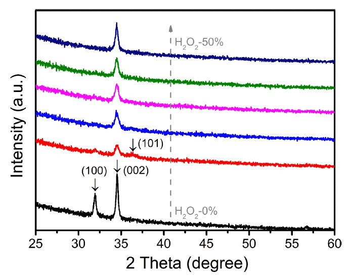
X-ray diffraction (XRD) patterns of ZnO–H2O2 thin films for different concentrations of H2O2 (0%, 10%, 20%, 30%, 40%, and 50%).
For the wurtzite-structure ZnO, the c-axis (002) plane has the highest stacking density and lowest surface energy, indicating that the (002) growth orientation is the thermodynamically favored and preferred orientation, theoretically.34) The mixture of (100) and (002) growth orientations in ZnO-H2O2-0% implies that the growth of the (002) plane is suppressed, for example, as a result of the adsorption of CH3− or CH3CH2−, which are dissociated from the ethyl groups of DEZ.35) This type of adsorption can be suppressed at high substrate temperatures by the resolution of CH3− and CH3CH2−, resulting in ZnO films with (002) plane growth orientation.35) A previous study had shown that H2O2 has a higher efficiency in cleaning the residual species in the ALD system than H2O.36) This can be another reason contributing to the change in the preferred growth orientation of ZnO, from mixed planes of (100) and (002) to a single (002) plane, upon increasing the H2O2 concentration.
3.2. Surface morphology properties
Figure 2 shows the FE-SEM images of the ZnO thin films prepared using different concentrations of H2O2. In the case of ZnO thin films, grains with the (100) and (002) growth orientations generally have wedge-shaped and column-shaped surfaces, respectively.33) As shown in Fig. 2, the ZnO-H2O2-0% sample has a mixed surface morphology of wedge-like and columnar (Fig. 2(a)). A transition of surface morphology to the (002) columnar-dominated morphology can be observed in the ZnO-H2O2-20% sample (Fig. 2(c)). Figs. 2(d) to 2(f) show the surface morphologies of the ZnO-H2O2-30%, ZnO-H2O2-40%, and ZnO-H2O2-50% samples, with complete and uniform columnar structures. The above results in the FE-SEM images are consistent with the XRD results in Fig. 1, and it can be inferred that the increase in the H2O2 concentration from 0% to 50% induces an increase in the oxygen concentration in the ALD chamber for ZnO thin-film growth. This oxygen-rich growth condition results in a growth orientation change to (002), depending on the surface energy.
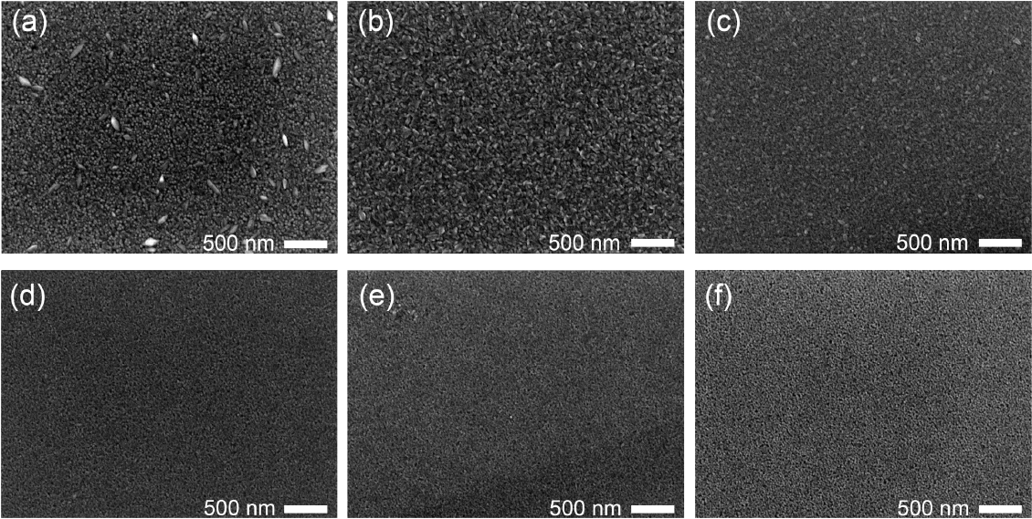
Field-emission scanning electron microscopy (FE-SEM) images of (a) ZnO-H2O2-0%, (b) ZnO-H2O2-10%, (c) ZnO-H2O2-20%, (d) ZnO-H2O2-30%, (e) ZnO-H2O2-40%, and (f) ZnO-H2O2-50%.
3.3. Photoluminescence properties
Previous studies had indicated that PL analysis is a useful method for studying defect types in ZnO. For example, it has been shown that the green emission at approximately 550 nm can be attributed to the presence of Vo and zinc interstitials (Zni),37–39) while the yellow emission at approximately 585 nm may be induced by oxygen interstitials (Oi) and Zni, and the orange-red emission from 600 nm to 750 nm may be attributed to the Oi and oxygen anti-sites (OZn).37–39) Therefore, to study the effect of different H2O2 concentrations on Vo in ZnO films, the PL spectra of all samples were analyzed at room temperature in the wavelength range from 300 nm to 700 nm. As shown in Fig. 3, two PL emission peaks were observed in all ZnO films. The emission peak located at approximately 375 nm could be attributed to the well-known UV near-band-edge (NBE) emission. The broad emission peaks in the range of approximately 540 to 630 nm could have been caused by the presence of oxygen and zinc-related defects such as Vo and Zni. Compared to the ZnO-H2O2-0% sample, the intensity of the broad emission peak (540 to 630 nm) was decreased remarkably in all ZnO–H2O2 films. Previous results had indicated that the use of H2O2 as an oxygen precursor could provide an O-rich growth environment and could passivate the formation of Vo.30,31) A decrease in the PL emission intensity at approximately 540 to 630 nm indicated a decrease in the oxygen and zinc-related defects. Additional analyses with the Hall properties of carrier concentration are provided in the next section. A slight increase in the PL intensity at approximately 540 to 630 nm, with the increase in the H2O2 concentration from 30 and 40% to 50%, could be explained by the increased film crystallinity, as shown in Fig. 1.40)

Photoluminescence (PL) spectra of ZnO films with different H2O2 concentrations.
3.4. Electrical properties
The as-prepared ZnO film normally has n-type characteristics because of the effects of the n-type Vo defects in ZnO, as similar to the other defects in semiconductors, the concentration of Vo in ZnO can also influence the electrical properties of the semiconductor ZnO. Previous studies had shown that the decrease in the Vo concentration in ZnO films, caused by post-annealing in oxygen atmosphere and increasing the oxygen partial pressure in the preparation process, could result in a decrease in the carrier concentration and increase in the resistivity.20,26) As a result, the use of H2O2 instead of ALD oxygen precursor H2O could inhibit the formation of Vo in the ZnO films.18,19) Therefore, the electrical properties of the ZnO film were investigated for different H2O2 concentrations. Fig. 4 shows the carrier concentration (a), Hall mobility (b), and resistivity (c) of the ZnO–H2O2 films for different H2O2 concentrations. With the increase in the H2O2 concentration from 0% to 50%, Fig. 4 (a) and (b) show a decrease in the carrier concentration and mobility (H2O2: 0% to 30%) followed by a slight increase in the mobility (H2O2: 30% to 50%). The decreased carrier concentration could be attributed to the decrease in the Vo and Zni concentrations, as the n-type defects in the ZnO film could serve as sources of carrier generation. The decreased carrier mobility in the ZnO films using H2O2, when compared to the ZnO-H2O2-0% sample with only H2O, could be attributed to a decrease in the film crystallinity, as shown in Fig. 1. A slight increase in the carrier mobility as the H2O2 concentration increased from 30% to 50% could be caused by the slight increase in the film crystallinity, as predicted in Fig. 1. Therefore, the use of H2O2 in the ALD oxygen precursor could lead to a decrease in Vo and reduce the carrier concentration. Fig. 4(c) shows that the resistivity of the ZnO–H2O2 films increases with the increase in H2O2 concentration due to the decrease in the carrier concentration.

(a) Carrier concentration, (b) Hall mobility, and (c) resistivity of the ZnO-H2O2 films for different H2O2 concentrations ranging from 0% to 50%.
4. Conclusions
ZnO thin films were prepared using the ALD method with DEZ and H2O2, with different H2O2 concentrations ranging from 0 to 50%. The results showed that some properties of the ZnO thin films changed upon increasing the H2O2 concentration from 0 to 50%. The growth orientation and surface morphology of the ZnO thin films changed, from coexistence of wedge-like (100) and columnar (002) planes to the existence of a single columnar (002) plane. The film crystallinity increased as the H2O2 concentration increased from 10 to 50%. The PL emission intensity at approximately 540 to 630 nm was clearly decreased. This could be due to the passivation of the n-type defects, most probably Vo and Zni. The changes in the PL intensity were related to the decrease in the carrier concentration and increase in the electrical resistivity. The passivation of n-type defects such as Vo and Zni in ZnO is helpful for the preparation of p-type ZnO with high carrier concentration and improved performance, which is suitable for use in ZnO-based devices.
Acknowledgments
This manuscript was based on the work “Development of Mott-transition based forming-less non-volatile resistive switching memory & array”, supported by the Ministry of Trade, Industry & Energy (MOTIE, Korea) under the Industrial Strategic Technology Development Program No. 10068075. Yue Wang thanks the China Scholarship Council (CSC) for financial support.