Design and Preparation of High-Performance Bulk Thermoelectric Materials with Defect Structures
Article information
Abstract
Thermoelectric is a key technology for energy harvesting and solid-state cooling by direct thermal-to-electric energy conversion (or vice versa); however, the relatively low efficiency has limited thermoelectric systems to niche applications such as space power generation and small-scale or high-density cooling. To expand into larger scale power generation and cooling applications such as ATEG (automotive thermoelectric generators) and HVAC (heating, ventilation, and air conditioning), high-performance bulk thermoelectric materials and their low-cost processing are essential prerequisites. Recently, the performance of commercial thermoelectric materials including Bi2Te3-, PbTe-, skutterudite-, and half-Heusler-based compounds has been significantly improved through non-equilibrium processing technologies for defect engineering. This review summarizes material design approaches for the formation of multi-dimensional and multi-scale defect structures that can be used to manipulate both the electronic and thermal transport properties, and our recent progress in the synthesis of conventional thermoelectric materials with defect structures is described.
1. Introduction
Research into renewable power generation sources has been received increasing attention due to the limits of conventional energy resources. Thermoelectric power generation (TEG) is highly beneficial as a power generation technology for efficient energy use because nearly two thirds of any energy consumed is ultimately lost via waste heat during energy generation and consumption processes. Moreover, TEG has a great potential to generate electricity especially from low quality heat (< 232°C, ~60% of unrecovered waste heat)1) and can increase the fuel efficiency of a vehicle. TEG systems also have the substantial advantages of no moving parts, compact size, and high reliability; however, there is no evidence that they have been used in large-scale waste heat recovery systems. One of the main technical barriers that restrict industrial application is the limited power generation efficiency of TEG modules, typically as low as 10% even in mid-to-high temperature systems,2–7) due to the low conversion efficiency zT (= σS2T/κ, where σ is the electrical conductivity, S is the Seebeck coefficient, κ is the total thermal conductivity, and T is the absolute temperature) of TE materials. The theoretical maximum power generation efficiency (ηmax) of a TEG device is given by the following equation:
where TH is the hot side TE leg temperature, TC is the cold side TE leg temperature, zTavg is the optimum zT value of the p- and n-type TE legs at average temperature (Tavg = (TH + TC)/2). To provide information about the relationship among the performance of materials (zTavg), efficiency of device (ηmax), and parameter of operating environment (ΔT), Fig. 1 shows the values of ηmax estimated with various zTavg by using equation (1) as a function of temperature difference (ΔT = TH − TC, TC = 300 K). As can be clearly seen in Fig. 1, for a given ΔT, a higher zTavg value resulted in a higher ηmax. A TEG device fabricated using TE materials with zTavg over 2.0 is required to realize an efficiency of ~ 22% when TH = 800 K (ΔT = 500 K).8) Considering that the maximum zT values of commercial TE materials such as Bi2Te3-, PbTe-, skutterudite-, half-Heusler- and Silicide-based alloys are remained at 1.0 – 1.2,9) the development of mass production scale materials with zTavg exceeding 2 is a great challenge. The main limiting factor in the development of conventional TE materials with high zT is the interdependency of the electronic (σ, S) and thermal (κ) transport properties. As shown in Fig. 2, semiconductors with low carrier concentration (n) have large S according to following relation, which is based on a parabolic band with energy-independenct scattering approximation10):
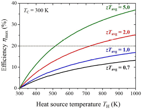
Thermoelectric conversion efficiency estimated as a function of zTavg and hot side temperatures of thermoelectric legs.

Schematic diagrams of (a) Seebeck coefficient (S), electrical conductivity (σ), and power factor (S2σ) and (b) variation of the thermal conductivity (κ) as a function of carrier concentration (n).
where kB is the Boltzman constant, e is the electron charge, h is the Planck constant, and m* is the effective mass of the carrier. However, low n also results in low σ (= neμ, where μ is the carrier mobility). Thus due to the trade-off relationship between σ and S, the power factor (σS2) values of typical TE materials can be maximized in an n range from 1019 to 1020 cm−3 (Fig. 2(a)).11) As shown in Fig. 2(b), thermal transport is also closely interrelated with n because of the electronic contribution of the charge carriers (electrons and holes) to the thermal conduction (κele = κ − κlat, where κlat is the lattice thermal conductivity determined by heat carrying phonons). A higher σ results in a higher κ because κele is determined by the Widemann-Franz law, κele = LσT. The Lorenz number L can be estimated using the following equation:
where r is a scattering parameter determined by the temperature dependence of μ, Fn(η) is the n-th order Fermi integral,
When the scattering mechanism is not well defined, L can be approximated using equation (5) proposed by Kim et al., where L is in 10−8 W Ω K−2 and S is in μV K−1.12)
From the above-stated electronic (σ, S, μ, r, m*) and thermal (L, κlat) transport parameters, the value of zT of TE materials can be enhanced by the following two approaches. The first approach seeks to enhance the power factor through modification of the band structure. The second approach, based on the PGEC (phonon glass electron crystal) concept for decoupling of the carrier and phonon transport, seeks to decrease κlat by promoting phonon scattering while the itinerancy of carrier transport.13)
2. Defects in Thermoelectric Materials
Defect engineering such as doping and nanostructuring for TE materials, by enhancing the power factor and/or reducing the value of κlat, has been shown to be one of the most effective routes to overcome the two trade-off relationships among the three TE parameters (Fig. 2). From recent theoretical and experimental considerations of TE materials with controlled defect structures, defects including 0-dimensional (0-D) point defects (impurity atoms, interstitials, vacancies), 1-D linear defects (dislocations), 2-D interfacial defects (boundaries such as grain boundaries, phase boundaries, and stacking faults), and 3-D bulk defects (inclusions) are central ingredients that can be used to control electronic and thermal transport properties.
2.1. 0-D Point Defects
A low κlat value can be obtained in amorphous solids due to the irregular arrangement of the molecules, such an arrangement is considered to be point defects for phonon scattering centers. Thus the formation of point defects via the introduction of foreign atoms is widely used for reducing the κlat value of TE materials. To maximize phonon scattering by point defects, three material design parameters, including (1) a high doping fraction, (2) a large mass difference between doping element and host atom, and (3) a large lattice mismatch between disordered and pure alloys, should be considered according to the Callaway model14) and following phonon scattering parameter (Γ ):15)
where, x is the doping fraction, ΔM/M is the rate of change of the atomic mass, ɛ is the elastic property, and adisorder and apure are the lattice constants of disordered and pure alloys, respectively. Thus, the value of κlat can be effectively reduced by increasing the doping fraction (density of point defects). Doping with multiple elements with different charge balance would be an effective way to increase the doping fraction since the single element doping, mainly due to charge imbalance, is limited by the low doping fraction. For example, a reduced value of κlat is obtained in Ga and Ag co-doped p-type Bi0.42Sb1.58Te3 due to the increased solubility limit of the doping elements.16) On the other hand, a reduction of κlat by increasing the rate of change of atomic mass can be attained by the formation of disordered vacancies as well as by substitutional doping.17) An extremely low value of κlat has been reported in partially filled CoSb3-based skutterudites which benefit from an intensified point defect phonon scattering due to the large mass difference (100%) between the fillers in filled CoSb3 and the vacancies in unfilled CoSb3.18)
The formation of 0-D point defect can also be used as an effective strategy to enhance the power factor by the modification of the band structure. In a degenerate semiconductor, S can be expressed by the Mott relationship:
where, E is the electron energy, is the carrier relaxation time, and EF is the Fermi energy. Thus, S can be enhanced by increasing the energy derivative of the DOS n(E) (the first term in equation (7)) near EF. An increase in DOS near EF is pursued based on point defect engineering for band convergence, resonant doping, and band flattening as shown in Fig. 3.19) The important role of band convergence (Fig. 3(c)) in zT enhancement can be well understood by considering the following dimensionless TE quality factor (B), which is directly related to zT at optimized n:19)

Schematic representation of the density of states of (a) a single valence band, (b) flattened band, (c) converged band, and (d) the introduction of resonant states.
where, h is the reduced Planck constant, Nv is the number of degenerated valleys for the band, Cl is the average longitudinal elastic moduli, mI* is the inertial effective mass, and Ξ is the deformation potential coefficient. According to equation (8), increasing Nv is one of several effective approaches to enhance the power factor, and one possible way to increase Nv is to converge different bands in the Brillouin zone, that is utilize convergence of bands, within a few kBT of each other. For example, the valence band at the L point (Nv = 4) and at the band along the ∑ line (Nv = 12) of PbTe can be converged by doping with several elements.20–22) Recently, power factor enhancement by band convergence effect has been experimentally proven for other TE alloys including doped Mg2Si23,24) and SnTe,25–27) however, in Bi2Te3-based alloys, the band convergence concept has not been sufficiently investigated because most previous experiments have assumed a single band model. Using the band convergence effect, further enhancement of S in Bi2Te3-based alloys is possible due to the high symmetry rhombohedral crystals, suggesting that there are multi-bands in the electronic structure.
Enhancement of the power factor via the introduction of point defects has also been seen in several TE chalcogenides such as Tl-doped PbTe,28) Sn-doped Bi2Te3,29) and In-doped SnTe,30) that is due to resonant states formation originating from the coupling between the carriers of the doping element (generally selected from the neighboring group of host atoms31)) and the band of the host alloy (Fig. 3(d)). Significantly enhanced zT values have been obtained by resonant doping in binary systems, however, the genuine difficulty in resonant doping for S enhancement is that one must find the right doping element and the right doping level at the same time in multi-elemental compositions of commercial TE materials. Thus, the development of new analysis methodology for direct observation of the resonant state is required for the effective screening of doping elements. Such an analysis technology would be able to verify the existence of a resonant state and yield, first, precise information about the doping element and its doping level. At that point, it will be possible to maximize the S through another elemental doping for Fermi level tuning given the occurrence of the resonant state. As a result, the formation of 0-D point defects can be an effective way to simultaneously enhance the phonon scattering and the carrier transport properties; however, the development of effective experimental or theoretical analysis tools for the prediction of the TE transport parameters32,33) is highly necessary to guide experiments and to understand the results.
2.2. 1-D Dislocations
Using the several parameters related to phonons, including heat capacity (C), velocity (v), total relaxation time (τtotal), and frequency (ω), the theoretical value of κlat can be estimated by using the following equation (9):
In polycrystalline bulks with complex defect structures, τtotal depends mainly on scattering from the normal (N) and Umklapp (U) processes, 0-D point defects (PD), 1-D dislocations (D), 2-D boundaries (B), 3-D inclusions (I), strains (S), and bipolaron (BP). Thus, in equation (9), the inverse τtotal is given as:
Figure 4 provides a schematic illustration of the heat carrying phonon distribution and of effective phonon scattering defects with different frequencies. Due to the frequency dependence of

Wavelength (frequency)-dependent phonon scattering mechanism related each individual defect structure.
Dense dislocation arrays at boundaries can also improve the electronic transport properties. Due to the low-energy states of semicoherent boundaries with dislocation arrays, carrier scattering can be significantly reduced and a higher value of μ can be obtained compared to that possible when using bulks with incoherent grain or phase boundaries. Thus, the formation of coherent or semicoherent grain and phase boundaries has been investigated as a solution to reduce the value of κlat, while maintaining the value of σ.41–44) However, due to the complexity of and differences in the electronic and thermal transport behaviors of each TE materials, detailed theoretical and experimental investigations, especially into the relationship between dislocations and the TE transport properties are required for further zT enhancement of commercial state-of-the-art TE materials.
2.3. 2-D Boundaries and 3-D Inclusions
As shown in equations (9) and (10), boundary scattering can reduce the phonon mean free path especially at low frequency (
where v is the average phonon velocity and d is the grain size. Thus the defect engineering of the nanostructuring for the production of nanocomposites consisting of nanograins (a nanograin composite) has been carried out as one of the main approaches to reduce κlat. The key idea of a nanograin composite is to utilize the high density of the grain boundaries to scatter phonons without significantly affecting the electronic transport properties. Nanograin composites of TE materials have been shown to be effective provided that the characteristic size of the nanograins is smaller than the phonon mean free path in the bulk materials. Reduced κlat values of commercial TE materials including Bi2Te3-,45–47) PbTe-,48,49) skutterudite-,50) half-Heusler-,51) and Si-Ge-based alloys52,53) have been reported in many studies via this approach. Another defect engineering approach of nanostructuring is the formation of multi-phase nanocomposites that contain a high density of secondary-phase nanoinclusions (a nanoinclusion composite). The nanoinclusions form two types of defect structures in the TE matrix (2-D phase boundaries and 3-D inclusions), which structures are able to reduce the value of κlat by effective scattering of mid-frequency phonons (Fig. 4). Generally, desirable sizes of nanoinclusions for phonon scattering range from several to dozens of nanometers. Uniform distribution is another key factor necessary to increase the phonon scattering effect by maximization of the interface density according to equation (12):54)
where σs is the scattering cross section at the short-wavelength limit, σl is the scattering cross section at the long-wavelength limit, and Vρ is the number density of nanoinclusions. Because the phonon scattering effect is intensified even at relatively low volume fraction of nanoinclusions, this nanoinclusion composite approach has been widely applied to various TE materials including Bi2Te3-,55–57) PbTe-,48,58–61) and skutterudite-based62–65) alloys.
On the other hand, according to the second term in equation (7), enhanced S can also be obtained in this nanoinclusion composite benefitting from carrier filtering effect due to the energy dependent modulation of the value of τ at the phase boundary between the TE matrix and the nanoinclusions. Our previous results on a model system of Te nanoparticle embedded Bi0.5Sb1.5Te3 thin films fabricated by pulsed laser deposition have proven that the carrier filtering effect is very effective at S enhancement; we obtained numerical design rules (size and fraction of nanoinclusions as a function of energy difference between TE matrix) for the maximization of the power factor.66) Combined with these material design considerations, the development of processing technology with ultimate controllability of processing parameters for the generation or introduction of nanoinclusions with precisely controlled characteristics (density, composition, size, and interface structure) in bulk materials can be used to realize a novel TE nanoinclusion composite with an enhanced zT by the simultaneous enhancement of the phonon scattering and the electronic transport properties. Further investigation into the high-temperature stability of nanoinclusions is also required due to possible diffusion of defect structures, which would reduce the effectiveness.
It is believed that the manipulation of defect structures triggers an enhancement in TE performance. Thus research into the development of simple and efficient synthetic techniques targeted for each commercial TE material has been inspired in an effort to generate the controlled and combined defect structures that can maximize the power factor and simultaneously minimize the value of κlat. In the following section, we introduce non-equilibrium synthesis techniques that are effective for the fabrication of TE materials with complex defect structures. Our newly developed processing techniques for defect engineering are also presented.
3. Processing Technologies for Defect Engineering
The formation behaviors of defect structures inevitably depend on the synthesis routes and processing parameters of the each of the fabrication steps. Defect structures with low energy can be easily formed in a TE matrix by using equilibrium synthetic processes such as melting and slow solidification, melt-solidification and annealing, and repeated solid state reactions; however, metastable or complex defect structures, which are central ingredients to enhance both the electronic and the thermal transport properties, cannot be attainable via these conventional processing technologies. On the other hand, non-equilibrium synthetic processes such as high-energy ball milling, rapid solidification process, and ultra fast sintering offer the opportunity to generate unexpected atomic- or nano-scale defect structures. In the following sections, we will summarize three non-equilibrium synthetic processes, that have more profound implications for a mass-scale production of high-performance TE materials: high-energy ball milling (HEM), melt spinning (MS), and spark plasma sintering (SPS).
3.1. High-energy ball milling
Besides the bottom-up chemical synthesis routes, high-energy ball milling (HEM) is another simple, effective, and productive way to prepare nanopowders, heterostructured nanopowders, and heterostructured nano/micropowders of TE materials. For example, nanograin composite of p-type Bi-Sb-Te with highly dense grain boundaries was fabricated by a combined technique of HEM of Bi-Sb-Te nanopowders and hot pressing for their compaction.47) This approach to the fabrication of nanograin composites of TE materials has been proven to be effective in reducing the value of κlat in commercial TE materials, as described in the previous section for 2-D boundaries.45–53)
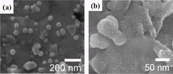
HEM can be also used to synthesize nano/nano and nano/micro heterostructured powders. Their bulks have a great potential to develop an enhanced value of zT due to the possible simultaneous effects of phonon scattering (reducing κlat) and carrier filtering (enhancing the power factor) in the presence of complex 2-D (highly dense grain and phase boundaries) and 3-D (nanoinclusions) defect structures (see section 2.3). However, well controlled complex defect structures, which are an essential factor in attempts to obtain a high zT, cannot be attained by simple HEM process. To address this, we used an HEM-based nanometal decoration technique (mixing and evaporation process for mixtures of Bi0.5Sb1.5Te3 and metal acetate powders), and obtained Bi0.5Sb1.5Te3 powders decorated with nearly monodispersed Cu nanoparticles (~50 nm, Fig. 5(a)).67) Very recently, we found that the size of Cu nanoparticles can be significantly decreased in value by about ~5 nm via control of the heat treatment conditions, as shown in Fig. 5(b).68) This simple and efficient approach to the fabrication of nanoscale heterostructured seed powders for an improved controllability of defect structures in bulks will be one of several epoch making techniques that will widen the applications of thermoelectrics. Another promising HEM-based heterostructuring technique is a combination of HEM with the chemical synthesis of boundary engineered TE nanomaterials (nanoparticles, nanoplates, and nanoflakes). Recently, we developed a successive epitaxial growth technique for the scalable synthesis of heterostructured nanoplates (Bi2Se3@Bi2Te3) and multishell nanoplates (Bi2Se3@Bi2Te3@Bi2Se3 and Bi2Se3@Bi2Te3@Bi2Se3@Bi2Te3) with a coherent phase boundary between Bi2Se3 and Bi2Te3.69) Well controlled complex defect structures in the bulks fabricated from the HEMed powders of boundary engineered heterostructured TE nanomaterials were found to provide an effective way to decouple the electronic and thermal transport.
Another promising use of HEM is a fast preparation method for the single phase of skutterudite-based alloys. Generally, due to a peritectic phase transformations, an ingot of filled skutterudite fabricated by conventional melt-solidification process contains various secondary phases including constituent elements and binary alloys.70–73) Thus, a long-time annealing process (~7 days), which is one of the main barriers to cost-effective materials preparation, is indispensable to obtain a single phase material with a high value of zT especially for multiple filled skutterudites.74) Recently, HEM has been used as a simple and efficient method to reduce the processing time.75) Formation of a nanoscale grain structure by HEM triggers a transformation into a filled skutterudite phase during the sintering process due to the significantly reduced distance that the fillers need to diffuse. A single phase bulk of Ce0.45Nd0.45Fe3.5Co0.5Sb12 has been achieved in 2 days via a combined technique of HEM and hot pressing.
3.2. Melt spinning
The melt spinning (MS) process is a conventional technique for the preparation of ribbons or flakes of alloys (or metals), in which a thin stream of a molten alloys contacts a rotated Cu wheel; cooling rates are in the range of 104 – 107 K s−1. Due to this high cooling speed, non-equilibrium or supersaturated phases of amorphous alloys such as bulk metallic glasses can be fabricated by using MS. Recently, MS has received renewed attention as one of the key processing technologies for defect engineering of TE materials because the phase formation and growth behaviors can be controlled by adjusting the composition of the starting materials and cooling rate. Additionally, quite different chemical and morphological features can be obtained along the growth direction (from the contact surface to the free surface, as shown in Fig. 6(a)) of ribbons due to the difference in cooling rates. For example, a multiscale microstructure was obtained in MS ribbons of Bi2Te3-based alloys. As shown in Figs. 7(a) and 7(b), a fine nanograin (~80 nm) structure is observed at the contact surface due to the high cooling rate, while a bundle of rod-like crystals with pores are present close to the free surface. This indicates that the structural sizes of the MS ribbons can be controlled by the cooling rate of the molten alloys, which is determined by the processing variables such as the Cu wheel rotating speed, the ejection pressure, and the temperature of the molten alloys. As can be seen in Figs. 7(b) and 7(c), a resultant strong dependence of the Cu wheel rotating speed on the thickness of the rod-like crystals at the free surface is observed. Due to this superior controllability of nanoscale defect structures, the MS process has been widely used for the preparation of seed powders to fabricate TE bulks with multi-scale and multi-dimensional defect structures. Nanograin and nanoinclusion composites of state-of-the-art TE materials have been achieved by combination of MS and a fast sintering technique such as hot pressing or SPS.76–82)
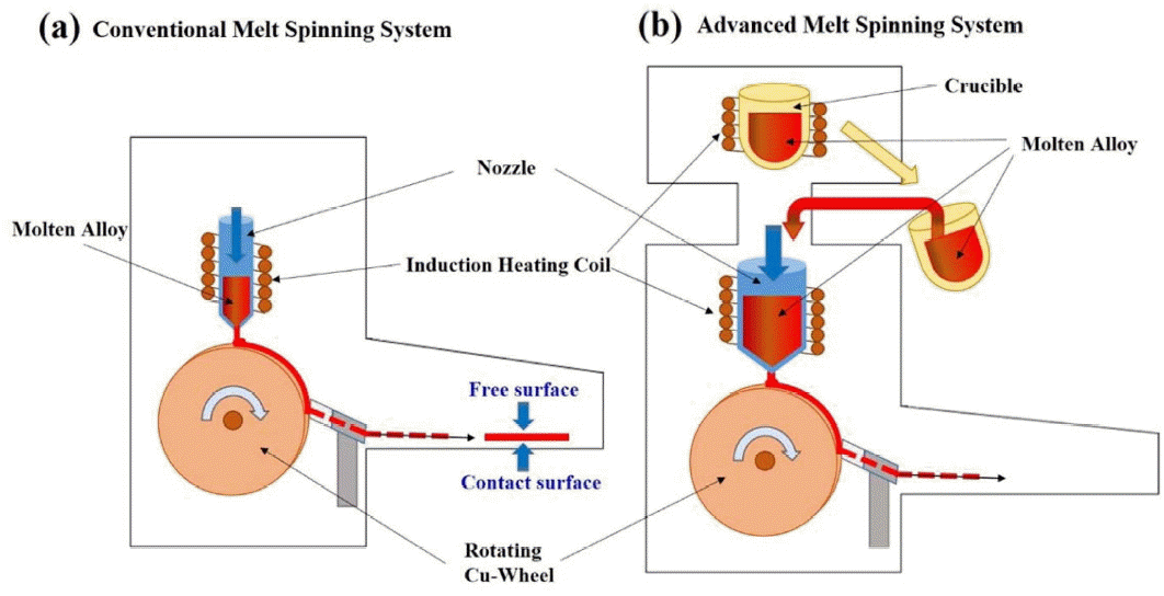
Schematic illustrations of (a) conventional melt spinning system and (b) advanced melt spinning system for up-scaled preparation of melt spun ribbons.
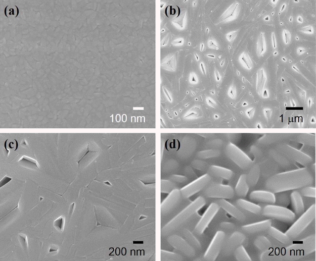
(a) Contact surface SEM image and (b) free surface SEM image of Bi0.5Sb1.5Te3 ribbon prepared by melt spinning fabricated at the linear Cu wheel rotating speed of 30 m s−1. (c) Free surface SEM image of Bi0.5Sb1.5Te3 ribbon prepared by melt spinning at fabricated at the linear Cu wheel rotating speed of 45 m s−1. (d) Free surface SEM image of heterostructured ribbon prepared by melt spinning at fabricated at the linear Cu wheel rotating speed of 40 m s−1 showing the Bi0.5Sb1.5Te3 platelets surrounded by the eutectic phase of Bi0.5Sb1.5Te3-Te mixture.
Pore structure formed at the free surface of the melt spun ribbons of the Bi2Te3-based alloys (Figs. 7(b) and 7(c)); this suggests that nanoscale heterostructures with high density phase boundaries can be fabricated by using appropriate mixtures as starting materials. Very recently, we successfully prepared heterostructured ribbons (Fig. 7(d)) of Bi0.5Sb1.5Te3 and eutectic phase (composite of major elemental Te and minor Bi0.5Sb1.5Te3 nanoparticles) from a mixture of Bi0.5Sb1.5Te3 and Te (~25 wt.% of Bi0.5Sb1.5Te3), and fabricated bulks with highly dense dislocation arrays at grain boundaries by using a SPS-based transient liquid flow assisted sintering process.38) This is a type of modified liquid phase sintering including the squeezing of the liquidified eutectic phase during pressure assisted sintering at a temperature (~480°C) between the melting points of Bi0.5Sb1.5Te3 (~620°C) and of the eutectic phase (~420°C). The generation of dislocation arrays along the grain boundaries is considered to be related with the accelerated grain rotation and rearrangement when the liquid phase is expelled. From these considerations, it can be said that the introduction of dense dislocation arrays into low-energy grain boundaries can also be achieved by a combination of a HEM process for the heterostructured nanopowders of Bi0.5Sb1.5Te3 and Te and a SPS process using the resulting powders. These engineered grain boundaries with dislocation core and strain (Fig. 8)38) can be utilized to enhance the zT value further by phonon scattering with a wider range of frequencies (see section 2.2). However, the detailed mechanism for the formation of dislocation arrays at grain boundaries during the transient liquid flow assisted sintering process should be clarified for further zT enhancement of Bi2Te3-based alloys and other state-of-the-art TE materials. Additionally, the effect of the processing parameters, especially to control the cooling speed, of the MS and SPS processes on the grain size and the density of dislocations should be investigated to confirm the reproducibility of the microstructure of the melt spun ribbons. This reproducibility will be critical factor for mass production. Fig. 6(b) provides a schematic illustration of our newly devised MS system for the up-scaled production of TE ribbons. As shown in Fig. 9, it was possible to fabricate large-scale (~500 g/batch) ribbons with highly reproducible and uniform composition and microstructure via the addition of parts for temperature regulated melting and continuous feeding of molten alloy.
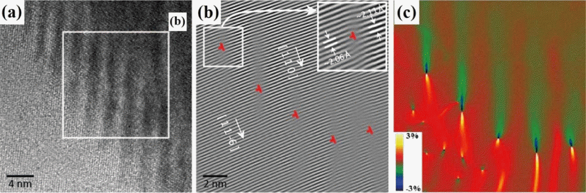
Dislocation arrays embedded in grain boundaries. (a) High resolution Transmission electron microscopy (TEM) image of a grain boundary. (b) Inverse fast Fourier transform (FFT) image with (11 −6) and (110) planes for the left and right grains, respectively, of boxed region in (a). (c) Strain mapping of (b), showing the dislocation cores with the high intensity.38)
3.3. Spark plasma sintering
Spark plasma sintering (SPS) is a consolidation technique that uses uniaxial pressure and a pulsed DC current to perform the compaction of the powders; this process is widely used as a rapid sintering method. By simultaneous application of pressure and temperature, a dense compact is obtained at a lower sintering temperature (~200 – 300°C) than is possible when using the conventional sintering processes. The intrinsic properties of TE powders with nanoscale defect structures can be maintained in their fully dense bulks because there are favorable sintering behaviors of less grain growth and suppressed powder decomposition due to the high sintering rate and low sintering temperature of SPS. Thus, nanograin and nanoinclusion composites of commercial TE materials can be easily fabricated by SPS without considerable grain growth.
SPS can also be used as an effective process for the generation of metastable phases and engineered boundaries because it allows the control of the diffusion reaction between grains with different compositions, thus SPS triggers the formation of multi-dimensional and multi-scale defect structures. However, several items should be addressed for any industrial application of SPS as a fabrication process for TE bulks with complex defect structures, including the following technical requirements: (1) precise control of sintering temperature and pressure, (2) increased ramping and cooling speed, and (3) automatic operation. One possible approach to solve the trade-off between precise temperature control and increased ramping speed is “hybrid heating”. Hybrid heating is a combination of the SPS process with other additional heating systems. The thermal gradient problem of SPS can be significantly improved by using an inversely directed gradient of an additional heating system; simultaneously, ramping speed is also further increased. Fast cooling is another important factor in the formation of a controlled defect structure. This can be realized via the installation of an additional cooling chamber with an automatic moving system of mold from the sintering chamber to the cooling chamber.
4. Summary
A review is provides here of the design and preparation of high-performance bulk thermoelectric materials with defect structures. Defect engineering approaches show promise as a means of enhancing the performance of thermoelectric materials by the simultaneous enhancement of phonon scattering and electronic transport properties. Novel bulk forms of commercial thermoelectric materials with complex defect structures have been demonstrated experimentally via a the combination of non-equilibrium synthetic processes such as high-energy ball milling, melt spinning, and spark plasma sintering. However, there are many more challenges to meet before it will be possible to establish the design rules for complex defect structures, and advanced processing techniques necessary to realize such structures and to attain a high value of zT. We believe that our perspectives will be highly beneficial for the development of novel thermoelectric materials, which can be used to secure the economic feasibility of thermoelectric power generation system as one of a main source of renewable energy.
Acknowledgments
This research was supported by the Basic Science Research Program through the National Research Foundation of Korea (NRF) funded by the Ministry of Education (Grant No. 2015R1D1A3A01018534) and the Industrial Fundamental Technology Development Program (10052977) the Ministry of Trade, Industry and Energy (MOTIE) of Korea.