


1. Introduction
One-dimensional (1D) piezoelectric nanostructures, due to the unexpectedly good performance of their size/geometry-dependent properties, have been studied as critical alternatives for next generation energy harvesting devices.1-3) There have been a lot of examples of promising nano-scaled harvesting devices that actually show better performance than that of corresponding thin films or bulk materials.4,5) Even up to the present moment, considerable progress has been made in achieving promising nanostructures using different growth techniques.6,7)
Chemical vapor deposition (CVD) via the vapor-liquid-solid (VLS) mechanism using nanoporous templates has been a competitive process because of the generally low processing cost.8-11) We recently demonstrated a CVD technique that used a magnetic field to prepare high quality GaN nanowires.12) This approach generates uniform alignment of nanowires without kinks and twists; this favorable outcome results from the interaction of magnetic field-guided Ni catalysts with vapor precursors. A few research groups have introduced magnetic manipulation of certain nanostructures.13-18) However, those studies used magnetic fields for post-growth alignment of the nanostructures, not during the formation/growth stage.
In this work, the piezoelectric energy harvesting characteristics of GaN nanowires grown using an external magnetic field through the VLS mechanism in a CVD setup have been investigated. There have been numerous research efforts to explore the possibilities of using GaN-based nanostructures for piezoelectric energy harvesting devices.19-23) For example, Lin et al.21) demonstrated a high output nanogenerator using GaN nanowire composite structures, with output voltage and output current density of 1.2 V and 0.16 μA/cm2, respectively. Chen et al.23) fabricated GaN nanowire nanogenerators having a maximum output power density of ~12.5 mW/m2. Wang et al.20) optimized the output efficiency of GaN nanowires by controlling the free carrier concentration with Si doping. In the present study, a ferromagnetic catalyst of Ni under the influence of fixed magnetic field strength was used for deposition at near-ambient working pressure. The morphology of the resultant GaN nanowires was changed by means of deposition time. Potential energy harvesting characteristics in terms of different types of GaN morphology are the main subject of this study. To the best of our knowledge, there has been no report demonstrating the dependence of the output current of GaN nanowires on dimensional changes of the nanostructure. Using this novel CVD technique, a noticeable maximum output current of ~14.1 nA is achieved for the 90 min-processed nanowires.
2. Experimental Procedure
The detailed experimental procedure for preparing GaN nanowires was described in our previous report, along with experimental evidence that explains the effect of the magnetic field according to different field strengths.12) Prior to the growth of the nanowires, a 10 nm-thick nickel layer was deposited as a catalyst on a Si (100) substrate by DC magnetron sputtering at 15 mtorr. For the growth of the GaN nanowires, trimethylgallium (TMG) as a source of Ga was vaporized at 750°C under gas flow of NH3/H2. The deposition was performed for different durations of 15 min to 90 min at atmospheric pressure. An AlNiCo permanent magnet having a Curie temperature of 850°C was placed on the top of the substrate prior to the deposition. The magnetic field strength was fixed here at ~ 0.80 T at room temperature.
The morphologies of the grown nanowires were observed by high resolution field emission scanning electron microscopy (FESEM: JSM-6300, JEOL). The phase of the nanowires was analyzed using an X-ray diffractometer (XRD: Max-2500, Rigaku), with Cu-ka radiation at l=1.5405 Å. The output current of the GaN nanowires was measured using a conductive atomic force microscope (c-AFM: Nanoscope V Multimode, Bruker) with a Pt/Ir coated silicon tip (PPP-NCHPt, NANOSENSORS). The tip has a pyramid shape with a 20~30° side angle. In the c-AFM contact mode, a constant normal force of 5 nN was maintained between the tip and the sample surface. Both the topography and the corresponding output current images were recorded simultaneously when the AFM tip was scanned over the nanowires with a scanning speed of 4 μm/s.
3. Results and Discussion
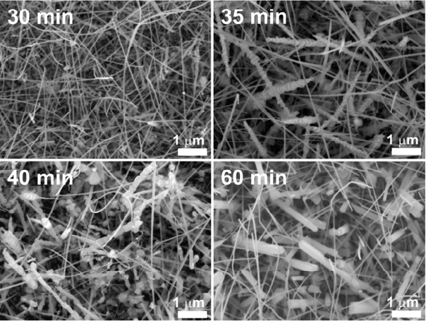
Microstructural characteristics of the GaN nanowires grown on the Ni-deposited Si substrate for different growth times can be seen in Fig. 1. The images clearly show that the dimensional features of the nanowires depend on the growth time. The morphology of the nanowires grown for 30 min was nearly uniform, with a smooth surface. The nanowires had diameters ranging from 40 to 60 nm, and were several micrometers long. As the growth time increased above 30 min, irregular shaped nanowires tended to be produced with enlarged width. The extended growth time up to 60 min resulted in substantially enlarged nanowires with a broader distribution in size. It seems that the growth time is a critical factor in determining the final morphology and uniformity of the grown nanowires. It may be not fully optimal to produce fairly uniform nanowires in width and length. The morphology is understood to be controlled additionally by the parameters of magnetic field strength, growth temperature, and thickness of Ni catalysts.12) However, as we will see later, nanowires with different widths may be good enough to define the capability of generating output currents because the values are coming from a single nanowire.
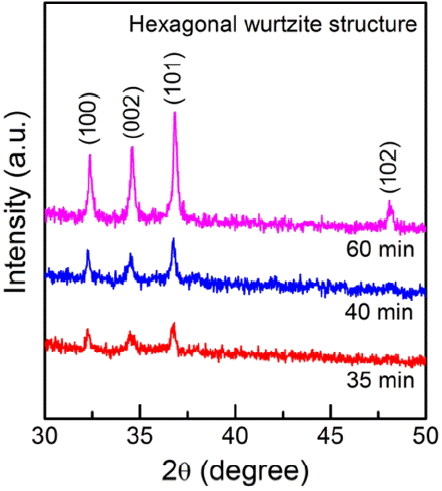
Figure 2 shows XRD patterns of the GaN nanowires grown for different times. The main diffraction peaks were identified as hexagonal wurtzite structure (JCPDS No. 50-0792). The peaks became more prominent with increasing growth time, indicating that strong crystallinity developed with prolonged growth time. It is interesting to observe the sensitivity of the crystallization to the growth time. It should be noted that no intense crystalline peaks of GaN were produced below the 30 min deposition time (not shown here). The randomized growth direction was identified clearly with the extended growth time of 60 min.
The output current value was characterized to suggest the performance of piezoelectric energy harvesting for the grown nanowires. Fig. 3(a) shows a three-dimensional plot of the output current, which was measured by c-AFM, for a selected 10 μm × 10 μm area in the nanowire sample grown for 90 min. The output currents are displayed with different color schemes that depend on the vertical height of each peak. The vertical axis corresponds to the output current. A tall peak, e.g., the red one, indicates a higher value of output current. Accordingly, the color distribution suggests the uniformity and level of output current over the designated area. The schematics shown in Fig. 3(b) indicate the simple mechanism of generating output current by AFM tip operation for a nanowire. The output current was obtained by direct measurement of the transient flow of electrons, which is driven by the piezoelectric potential in a GaN nanowire when the AFM tip operates in contact mode.19)
Figure 4 provides examples of the output currents generated for the 35 and 60 min samples when the AFM tip scanned over a line of 10 mm length. Each output current peak corresponds to a value for an individual nanowire. The negative value of the measured current indicates that the piezoelectric potential is driven by electrons.24) Some positive piezoelectric potential may exist in a bent nanowire, even though we expect the contribution of the positive value to be too small to overcome the reverse-biased Schottky barrier between the Pt/Ir coated tip and the nanowire. As expected, the 60 min sample demonstrates higher negative output currents than those of the 35 min sample, reaching the largest value of 13.6 nA (Fig. 4(b)). The value distribution is assumed to be directly related to the width of each nanowire. A thicker nanowire must have a larger value of output current.
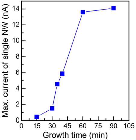
Figure 5 shows the maximum output current values obtained for samples processed at different growth times. The values increased slightly as the growth time increased to 30 min, and then increased rapidly with further increases of growth time to 60 min. The largest value of maximum output current reached ~14.1 nA for the sample grown for 90 min. Generally, along the piezoelectric semiconductor nanowire the potential (Vs±) distribution induced by the piezoelectric effect can be expressed by the following equation:25)
where e33, k0, kr, a, L, and γm are the piezoelectric constant, the permittivity of vacuum, the relative dielectric constant, the diameter of the nanowire, the length of the nanowire, and the maximum deflection of the nanowire, respectively. As the growth time increased, the large ratio of a/L can likely be attributed to the progressive growth of nanowires in the lateral direction. The lateral growth of the nanowires (or thicker nanowires) is associated with the limited usefulness of the Ni catalyst.12) In conclusion, the increase in the output current is believed to be due to the increased difference in the potential (or charge) distribution across the enlarged width of the nanowire. The enhanced crystallinity observed in the XRD pattern in Fig. 2 must also be responsible for the increased output current.
Because a different circuit system is used, it is difficult to compare the highest obtained output current of a single nanowire in this study directly to the output performance found in the literature. According to a simple estimation, however, our system is estimated to have the capability to produce ~7 V when we consider a typical resistance of 500 MΩ. This estimated voltage value is considerably higher than the reported values.25-27) For example, the obtained output voltage of a single nanowire was around 1 V for the 5 μm long and 25 - 100 nm thick nanowires.27) In this study, we assumed that the estimated output voltages would be 0.77, 2.29, 2.94, 6.80, and 7.05 V for the 30, 35, 40, 60, and 90 min-processed nanowires, respectively.
4. Conclusions
The parameter of growth time in the preparation of GaN nanowires by magnetic field-assisted CVD process turns out to be a determining factor in controlling the morphology and crystallinity of the GaN nanowires. The use of different morphologies and levels of crystallinity resulted in an enhancement of the piezoelectric energy harvesting performance. Thicker nanowires induced by extended growth conditions exhibited a higher value of output current. For example, the maximum value of a single nanowire processed for 90 min was ~14.1 nA, which corresponds to ~7 V. This suggests that GaN nanowires, with further optimization, can likely serve as even better energy harvesters.