1. Introduction
Aluminum nitride (AlN), whose theoretical thermal conductivity is 320 W/mK, is being used for electrostatic chucks and heaters in the semiconductor industry. In such applications, in addition to the need for a high thermal conductivity, the electrical conductivity of the ceramics must be well-optimized because their working mechanism depends on an electrical current under a high electrical field.1-6)
The oxygen content of approximately 0.8 wt% inherent to commercial AlN powder is mostly removed from the AlN grains through the forming of grain boundary precipitates with sintering additives such as Y2O3 and CaO.4,5,7) As described by Slack et al.,8) the remaining oxygen incorporates into the AlN grains by the following reaction
The oxygen defects, substituting for nitrogen ion sites, and the aluminum vacancies were believed to control the electrical and thermal conductivity.9-11) It was proposed that the aluminum vacancies are the charge carriers for AlN ceramics.9-11) This conclusion came from complex impedance spectrum studies with respect to temperature. Those studies, however, did not consider the effects of minor impurities such as transition metal oxides. Recently, TiO2 was reported to have a very strong effect on the electrical properties of AlN ceramics;12,13) the mechanism for this, however, has not been explained yet.
In this study, the electrical conductivities and impedance spectrums of 1 wt% Y2O3-doped AlN ceramics have been measured with respect to the additional TiO2 dopant. Microstructures of the sintered specimens were characterized through high-resolution transmission electron microscopy (HRTEM), and elemental analysis of the grain boundaries were conducted using scanning transmission electron microscopy (STEM). Based on the observed results, the implications of using AlN as an insulator have been discussed.
2. Experimental Procedure
Commercial AlN powder (F-grade, Tokuyama Soda, Japan) was used. According to the manufacturer’s data, the powder’s major impurity is 0.8 wt% oxygen, while other metallic impurities were present at levels of less than 10 ppm. As a sintering aid, 1 wt% of Y2O3 (grade C, H.C. Starck, Germany) was mixed with the AlN powder. TiO2 dopant (99.9%, Showa, Japan), at levels ranging from 0.05 wt% to 1.0 wt%, was also added to the AlN powder. The proportioned mixtures were ball-milled with an anhydrous ethyl alcohol medium in Teflon jars for 20 h. The resultant slurry was dried in an oven at 90°C for 24 h and then hot pressed in a graphite furnace at 1700°C for 3 h under applied pressure of 15 MPa.
Insulating properties were measured using the guarded electrode method based on ASTM D25714) under an electrical field of 500 V/mm and after a charging time of 60 seconds. Complex impedance spectrums were obtained between 150°C and 350°C using an impedance analyzer (1260, Solartron, UK) and a dielectric interface (1296, Solartron, UK) at a voltage of 1 V. Electronic conductivity was measured at a constant voltage of 1 V/mm using a source meter (617, Keithley, USA). Measured impedance spectrum was fitted using the software Zview (ver. 3.1, Scribner Asso., USA). Before the experiments, a silver paste was applied as an electrode and the specimens were annealed at 850°C for 20 min in nitrogen atmosphere. Microstructural characterization and elemental analysis were conducted using HRTEM (JEM-4010, Jeol, Japan) and STEM (JEM-2100F, Jeol, Japan). For the TEM analysis, the specimen was thinned and ion-milled following the conventional techniques of sample preparation.
3. Results
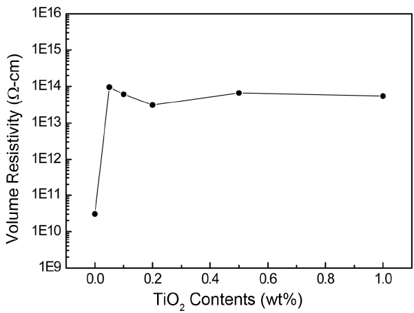
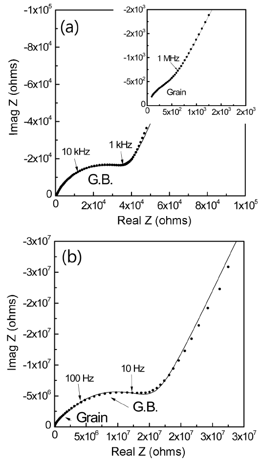
Figure 1 shows the electrical resistivity measured with respect to the added amounts of TiO2 after a charging time of 60 seconds in an electric field of 500 V/mm. Even with a 0.05 wt% addition of TiO2, the resistivity increased more than 1000 times. This high resistivity was maintained with further addition of TiO2. To understand this behavior, impedance was measured with respect to frequency. Fig. 2 shows a typical example of impedance spectra for AlN specimens with 1 wt%Y2O3 sintering aid and with an additional 0.05 wt% of TiO2 as a dopant. Impedance spectra consisted of three semicircles, as was found in the literature: 10,11) a semicircle due to grains at high frequency, a semicircle due to grain boundaries at low frequency, and a big semicircle from electrodes at the lowest bound of frequency. In the AlN specimen without TiO2 dopant, the resistance of the grain is much lower than that of the grain boundary. But, with TiO2 dopant at a level of 0.05 wt%, the grain resistance increased about 2500 times, while the grain boundary resistance increased about 380 times. The grain conductivity of AlN ceramics is known to be mostly ionic, with Al vacancy as a charge carrier.9-11) Thus TiO2 addition must affect the migration of Al vacancies.
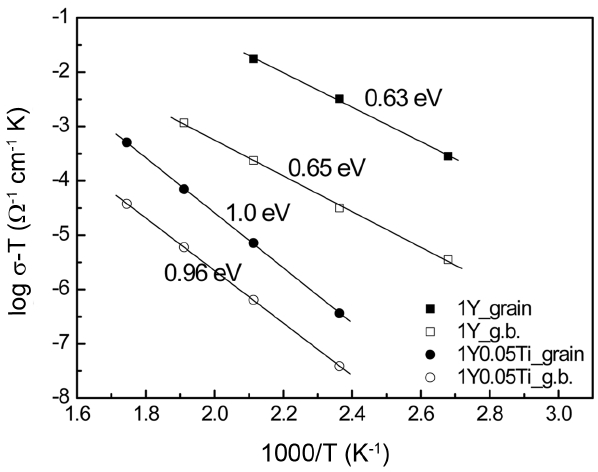
Figure 3 shows the conductivity changes of the grains and grain boundaries at various temperatures for the above two specimens. Over the investigated temperature range, the specimen with TiO2 dopant showed much lower conductivity than that without dopant. In the specimen without TiO2 dopant, the activation energy of the grain and the grain boundary were very similar, at 0.63 and 0.65 eV, respectively. However, in the specimen with TiO2 dopant at a level of 0.05 wt%, the activation energies increased to 1.0 and 0.96 eV for the grain and grain boundary, respectively. Thus, TiO2 addition induced not only a reduction in conductivity but also an increase in the activation energy.
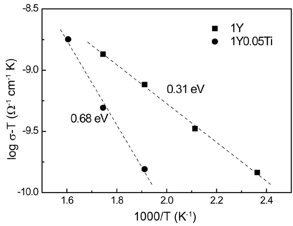
Figure 4 shows the electronic conductivity measured at 1 V/mm after a prolonged holding time. Because we used silver as the electrode material and because the measurement temperature was low, the ionic current must be blocked at the electrodes due to limited interface reaction, and thus only electronic current is allowed. Therefore, after prolonged application of DC voltage, a steady-state in electronic conduction would be reached, while ionic conduction would be totally blocked. In fact, we conducted very long experiments, for at least 2000 seconds, and then applied a longterm approximation to obtain the steady-state the electronic current. As the ionic conduction, electronic conduction also decreased with the addition of TiO2. The magnitude of the difference between these two samples was not as large as that in the case of ionic conduction. However, the activation energy change showed similar behavior; TiO2 addition increased the activation energy of electronic conduction by 0.37 eV.
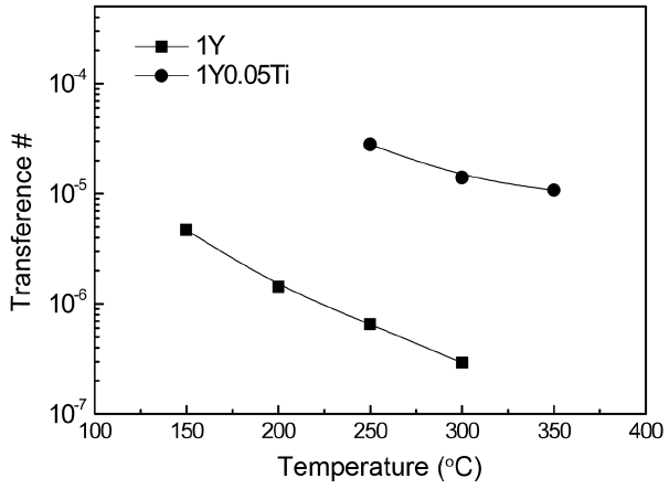
From the measured values of ionic and electronic conductivity, we were able to obtain the electronic transference number, which is the ratio of electronic to total conductivity (Fig. 5). Because ionic conductivity is much higher than electronic conductivity, we assumed that the sum of the grain and grain resistances were the total resistance, from which the total conductivity could be obtained. For both specimens, the electronic transference numbers were very small, in the range of 10−4 to 10−7, indicating that AlN ceramics are a predominantly ionic conductor at the measurement temperature range. With the addition of TiO2 dopant, the electronic transference number is higher because the reduction of ionic conductivity was much greater than the reduction of electronic conductivity, as shown in Figs. 3 and 4. The number decreased further with increasing measurement temperature because the activation energy of ionic conduction was higher than that of electronic conduction.
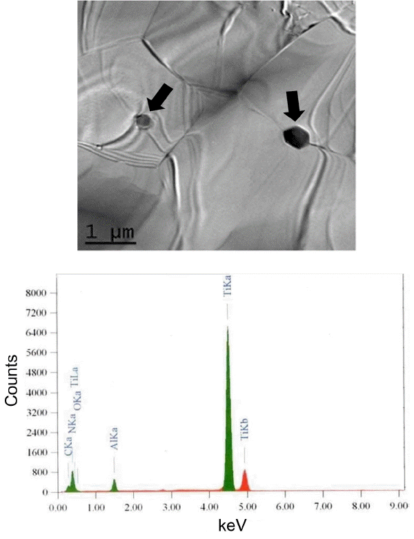
To understand this behavior, we observed the microstructure through TEM. For the specimen with 1 wt% TiO2 dopant, we found very small particles related to TiO2 addition inside the grain and along the grain boundary, as shown in Fig. 6. From the EDX analysis, it can be seen that this material has a composition close to Ti0.95Al0.5N, which means that the added TiO2 reacted with AlN to form nitride particles. However, inside the AlN grains, we found that Ti concentration was below the detection limit of EDX, indicating that Ti has very low solubility in AlN. TiN is known as a conducting material. However, in this case, the particles that were formed inside the grain and along grain boundary were not connected to each other, and thus they did not make a conduction path along the Ti0.95Al0.5N particles. The formation of Ti0.95Al0.5N particles from TiO2 also seems to contribute to an increase in oxygen content in the AlN grains. This additional oxygen from TiO2 resulted in a decrease in the thermal conductivity of the specimens from 92.5 W/mK without TiO2 addition to 77.6 W/mK with addition of 1 wt% TiO2.
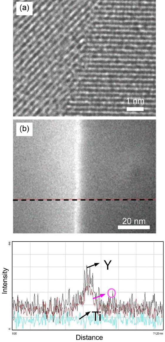
In order to check the atomic scale segregation along the grain boundary, we observed the grain boundary at high magnification and performed EDX analysis across the grain boundary (Fig. 7). As was found in the literature,11) we found Y segregation along the grain boundary, but there was no evidence of Ti segregation. The fact that the grain boundary conductivity was much lower than the grain conductivity might be attributed to this Y segregation. The result, that Y segregation in Al2O3 was determined to form more ionic bonds, may be related to this phenomenon.15)
From the above TEM analysis, we suggest that most of the Ti resulting from added TiO2 remains as Ti0.95Al0.5N particles along the grain boundary; only a very small fraction was incorporated into the AlN grains. This is consistent with the calculated phase diagram for cubic TiN and AlN.16) Though cubic AlN was considered instead of Wurtzite AlN, the solubility of TiN in AlN was very low.16) However, that low solubility was sufficient to have an impact on the ionic and electronic conductions, as shown above.
4. Discussion
In order to understand effects of TiO2 addition on the electrical properties of AlN ceramics, we have to first understand how Ti ions are located inside the AlN lattice. Using TEM analysis, we found a very small solubility of Ti in AlN grains. When we consider the ionic sizes of Ti and Al ions (0.61 Å for Ti4+, 0.67 Å for Ti3+, and 0.54 Å for Al3+),17) the size difference between the Ti and Al ions is relatively large: 13% in Ti4+ and 24% in Ti3+. Thus Ti ions inside the AlN lattice will probably prefer a +4 valence instead of a +3 valence, resulting in an effectively positive charge of a Ti ion in an Al site.
Conductivity is proportional to carrier concentration and its mobility. Because dopant concentration is very small inside the lattice, we may assume that the mobility of the Al vacancies is not affected. However, the carrier concentration should be considered in terms of thermodynamic aspects. A Ti ion with the effective positive charge can form an associate with negatively charged Al vacancy, as in:
The activation energy difference of the grain conductivity with the addition of TiO2, 0.37 eV, must stem from the binding energy of the association of two ionic defects. Similarly, an association between an electron and a Ti ion is also possible. Ti can be a redox center; however, in this case, the size of the Ti3+ ion after the reduction is too large for it to be accommodated at the Al site. Therefore, instead of the traditional reduction process, in which the valance changes with the accepting of an electron, electrons appear to be loosely bound to Ti4+ ions with a binding energy.
Activation energies of grain and grain boundary were very similar in each specimen. This can be attributed to the similar structural or electrical environment of grains and grain boundaries. Another possibility is a current-constriction effect coming from lateral inhomogeneity in the specimen or nonideal contact of the electrode. In such cases, the activation energy from a semicircle in the lower frequency range must be the same as that from the bulk.18) However, it is not clear which mechanism is responsible for the identical levels of activation energy; this point will need further investigation.
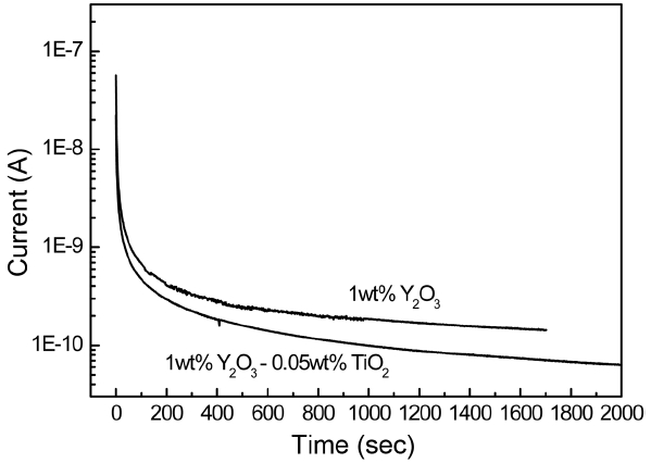
On the other hand, the very low electron transference number of AlN ceramics regardless of Ti addition means that AlN is predominantly an ionic conductor. This effect appears in the current variation with the time at constant DC voltage, as shown in Fig. 8. Because the measurement temperature is low, the exchange reaction of ions in the electrode must be very limited. So, the silver electrode is believed to effectively block the ion transfer in the electrode. Thus, the initial current at t = 0, which is contributed to by both ionic and electronic carriers, is high and decreases abruptly at the beginning and then slowly with time. The steady-state current is obtained as Al vacancy concentration profiles develop inside the specimen. The kinetics can be determined by a chemical diffusivity of AlN ceramics. The chemical diffusivity Dδ is expressed as19)
where te, tion, De, and Dion are the transference numbers and diffusivities of electrons and ions, respectively. In our case, tion (= 1 − te) is nearly one, and thus the chemical diffusivity can be simply expressed as
Therefore, from the relaxation time of the exponential current decay at constant voltage, we can obtain the diffusivity of the electrons and the electron concentration can be theoretically calculated using the Nernst-Einstein relation.20) However, this procedure to obtain the electron concentration requires us to be very cautious because electron trapping and grain boundary effects should be considered.21) A rough calculation shows that the electron concentration is on the order of 1012/m3, which is very low compared to the values of typical ceramics.
The facts that the electron transference number te is close to zero and the electron concentration is also very low compared to that of ionic carriers in AlN ceramics have an important implication in the application of AlN ceramics. For instance, when a voltage is applied in an AlN heater used in a CVD equipment, electric insulation does not occur until a certain incubation time is reached because the initial current established by the ions is significant. Second, even if the voltage is turned off, current can flow in the opposite direction due to a restoration to the equilibrium concentration profile of the Al vacancies from the profile developed during the voltage application. Both kinetics depend on the chemical diffusivity, which can be approximated by the electron diffusivity in AlN ceramics, for which the ionic transference number is close to one. In an application of an electrostatic chuck, the kinetics can also affect the practical chucking and dechucking times of wafers. If the electron diffusivity is high, then the chucking and dechucking times can be reduced because the current decay, as shown in Fig. 8, can be faster. Also, an AlN substrate in a power device package that operates at high voltage may show effects of current surges when high voltage is applied.
5. Conclusions
The electrical properties of AlN ceramics have been analyzed with respect to TiO2 dopant addition. TiO2 addition greatly decreased grain and grain boundary conductivities. With the TiO2 dopant, the activation energy of the grain conductivity increased about 0.37 eV; this increase was attributed to the formation of an associate between Al vacancies and Ti ions at the Al site. Similarly, the electronic conductivity was reduced with TiO2 addition, but the extent of reduction was not as great as the extent of reduction of the ionic conductivity. The activation energy for electronic conductivity increased similarly by about 0.37 eV. The TiO2 solubility in AlN grains was very low, below the detection limit of typical EDX analysis. Grain boundary was clean, without liquid film, but it showed yttrium segregation. The transference number of ions was close to 1, showing that AlN ceramics are predominantly ionic conductors. This was confirmed again by considering the current variation at constant voltage. This current variation with time can be understood with respect to the electron diffusivity.


