Development of Colloidal Quantum Dots for Electrically Driven Light-Emitting Devices
Article information
Abstract
The development of quantum dots (QDs) has had a significant impact on various applications, such as solar cells, field-effect transistors, and light-emitting diodes (LEDs). Through successful engineering of the core/shell heterostructure of QDs, their photoluminescence (PL) quantum yield (QY) and stability have been dramatically enhanced. Such high-quality QDs have been regarded as key fluorescent materials in realizing next-generation display devices. Particularly, electrically driven (or electroluminescent, EL) QD light-emitting diodes (QLED) have been highlighted as an alternative to organic light-emitting diodes (OLED), mostly owing to their unbeatably high color purity. Structural optimizations in QD material as well as QLED architecture have led to substantial improvements of device performance, especially during the past decade. In this review article, we discuss QDs with various semiconductor compositions and describe the mechanisms behind the operation of QDs and QLEDs and the primary strategies for improving their PL and EL performances.
1. Introduction
Solution-processed electrically driven quantum light-emitting diodes (QLEDs) have attracted much attention in research and in the display industry (e.g., Samsung, Sony, TCL, etc.) as they are one of the most promising candidates for next-generation displays. QLEDs have a device structure similar to that of organic LEDs (OLEDs); the only difference is that the emitting layer (EML) consists of quantum dots (QDs) rather than an organic material. QLEDs show important advantages over OLEDs, including narrow emission line widths and high stability against oxygen and water compared to organic materials. In particular, the saturated emission colors of QDs allow QLEDs to effectively reproduce the BT 2020 standard color parameters used for ultra-high definition television systems.1–5) Displays adopting QD technology have already been commercialized by cooperation between companies specializing in QDs and displays; however, this technology is based on color conversion methods in which QDs are used to convert the blue light from LED chips into different colors. In addition, this technology has been applied to a backlight unit in a liquid crystal display (LCD), and, except for the color reproducibility, has been found not to be competitive with the overall performance of OLED technology in such areas as response time, contrast ratio, and viewing angle. To improve the competitiveness of QD-based display technology and further realize flexible and transparent devices in the future, displays based on the above electrically driven QLEDs are thought to be a good solution.
In the early 1980s, Russian solid-state physicist Alexey I. Ekimov first discovered nano-scale semiconductors in a glass matrix.6) Later, Luis E. Brus in Bell Labs suggested that the size and band gap of semiconductor nanocrystals were interrelated;7,8) since then, the scientific evolution of QDs has progressed for more than three decades. The unique property of QDs, the ability to easily tune their band gap by controlling the particle size, has received interest from a diverse range of fields that use semiconductors, for applications such as field-effect transistors,9) solar cells,10) and light-emitting materials.1–5) In particular, the ability to vary the emission wavelength from ultraviolet (UV)11) to near-infrared (NIR)12) is a sufficient condition for using QDs as fluorescent materials; however, QDs in their early stage of development had little merit due to their low quantum yield (QY) and stability. After enhancing QD characteristics through continuous studies, researchers have applied QDs to lighting materials, where the two major types use the photoluminescent (PL) and electroluminescent (EL) properties of the QDs. EL from QDs in an LED platform was first reported in 1994; however, the external quantum efficiency (EQE) of the device was low (0.01%).13) Building on these findings, many studies investigating QLEDs have been undertaken and the EQE of the device has been dramatically improved up to ~ 20%.14,15)
The advancement of QLED technology has been accomplished by optimizing materials and structures. Hence, in this review article, we focus on summarizing the development of QLEDs over the past two decades and speculate on directions for the future. In Section II, we discuss QDs with respect to the basic principles, structures, and compositions. In addition, we present the properties of some common QD compositions (e.g. CdSe, InP, and CuInS2 (CIS)). Then, in Section III, we analyze the factors affecting QLED performance and show the characteristics of devices using different families of highly luminescent QDs. Finally, in Section IV, we conclude the review by discussing future prospects of these materials.
2. An Overview of QD Development
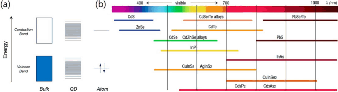
Semiconductor nanoparticles or QDs are composed of hundreds to thousands of atoms and have properties different from those of bulk materials; for example, they exhibit an intermediate electronic state structures between those of atoms and a bulk semiconductor (Fig. 1(a)).16) This is due to the quantum confinement effect that occurs in QDs, whose size is smaller than their exciton Bohr radius (the distance between electron- and hole-forming excitons, determined by Coulombic interaction). Confined excitons in three spatial dimensions lead to quantized continuous energy bands in the bulk semiconductor; as a result, the electronic band structure of QDs has discrete electronic states that are strongly size-dependent.7,8) Through this effect, the band gap energy of QDs increases as their size decreases; hence, the emission wavelength of QDs can be tuned simply by varying their size.17,18) Fig. 1(b) shows the spectral emission range of various kinds of QDs. Cd-based, InP, and CIS QDs cover the visible light range and have hence been intensively investigated as fluorescent materials.19)
2.1. Synthesis of high-quality QDs
To develop high-quality QDs for applications, the synthesis of colloidal QDs with a narrow size distribution is critical, and controlling the nucleation and growth steps in the synthesis process is especially important. The best condition for monodisperse QDs is fast nucleation followed by slow growth.18) Typical synthetic methods for QDs are heating-up20,21) or hot-injection.22–24) In the heating-up method, all materials needed for the synthesis, such as the anion and cation precursors, solvent, and ligands are placed together in a reaction flask and heated to the target temperature. This thermal treatment decomposes the anion and cation precursors; then, nucleation and growth of the nanoparticles begins (Fig. 2(a)). In Fig. 2(b), a schematic of the hot-injection method is illustrated. At the beginning of this procedure, only one of the precursors (either anion or cation) is mixed with the solvents and ligands in a reaction vessel, followed by heating to high temperature. Then, a solution containing the other precursor is swiftly injected into this hot solution, resulting in nucleation by supersaturation. The following growth stage proceeds through diffusion-controlled growth, in which the larger particles in the reaction solution grow more slowly than the smaller ones.25) Hence, the average particle size increases over time and QDs with a narrow size distribution are achieved. This nucleation and growth stage can be controlled by the precursor concentration, reaction temperature, and ligands. The synthesized QDs are then usually purified before being used for the intended application.

Synthetic approaches for QDs; (a) Heating-up and (b) hot-injection methods.
2.2. QD structures
QDs commonly consist of a core, shell, and organic ligands. The cores of the QDs are the emission centers, and mainly determine the emission wavelength and full-width-at-half-maximum (FWHM). Since QDs have an average diameter of only a few nanometers, the surface-to-volume ratio is very high. Hence, the characteristics of QDs are affected by surface trap states generated by dangling bonds and defects on the surface. The defect states in the electronic energy level structure of QDs trap excited electrons or holes and cause non-radiative decay, deteriorating the optical properties of the QDs.26–28) Hence, bare QDs without a shell exhibit low luminescence efficiency and poor stability, and are sensitive to changes in the surrounding environment. To reduce the number of dangling bonds on the core surface and improve the QD characteristics, core/shell heterostructures have been developed.29) Various types of core/shell heterostructures have been studied and use of these structures has led to significant improvements in the quality of QDs with respect to PL QY and stability.
The core and shell materials of the heterostructure are typically different semiconductors, where the different types of structures can be classified by the relative positions of the band gaps of the respective materials (Fig. 3(a)). First, a type I structure has a shell material with a band gap wider than that of the core. In this structure, both electrons and holes are confined to the core; for example, there could be a CdSe core and a ZnS shell. Fig. 3(b) shows the energy levels of semiconductor materials commonly used in QDs. The energy levels of a CdSe/ZnS QD show large offsets between the conduction band minima (CBMs) and the valence band maxima (VBMs). This offset acts as an energy barrier to prevent charge carriers from leaking from the core to the shell, resulting in an increased probability of exciton generation. In addition, surface passivation by the shell reduces the number of dangling bonds and defects on the surface of the core material. The optical properties of QDs can be enhanced via an increase in the probability of exciton radiative recombination. Hence, many QDs for high-quality fluorescent materials have adopted a type I core/shell structure.20–22,29)

(a) Schematics of the energy level alignments and carrier localizations in type I, reverse-type I, type II, and quasi-type II core/shell QDs. Red and blue lines indicate electron and hole wave functions, respectively. (b) Electronic energy levels and lattice constants (red dot) of various semiconductor materials.
Structures with energy level positions opposite to those of type I core/shell QDs, called reverse type I structures, have also been reported.30–32) Unlike the type I structure, in the reverse structure the charge carriers are partially or totally confined to the shell. For example, ZnSe/InP QDs having this structure show a phenomenon in which the peak PL wavelength changes from 430 to 610 nm with increasing thickness of the InP shell (narrower band gap) on the ZnSe core (wider band gap). The addition of a ZnS shell on the ZnSe/InP QDs was shown to also influence the PL properties, improving the PL QY and resulting in a red-shifted wavelength due to the complete localization of charge carriers in the InP region and surface passivation.30)
In type II structures, either the CBM or VBM of the shell material is situated within the band gap of the core material; this band gap alignment causes spatial separation of electrons and holes. Typical examples of structures with staggered energy level positions are CdSe/ZnTe33) and ZnTe/ZnSe QDs.34) In the case of CdSe/ZnTe QDs, electrons are localized in the core and holes move to the shell region. This phenomenon makes the QDs suitable for photovoltaic applications.33,34)
Lastly, quasi-type II structures have a core/shell system with a large band energy offset for one of the charge carriers and a very small offset for the other. CdSe/CdS QDs35,36) are an example of such a core/shell structure; they show a large offset of VBMs between the CdSe core and the CdS shell, while the offset of the CBMs is not sufficient to confine the electrons to the core. Hence, the hole wave function is confined to the core, while the electron wave function is delocalized over the core and shell. Due to this band offset structure, the PL properties of the QDs, such as the absorption and emission wavelength, shift to lower energy with increasing shell thickness, and the electrons in the CdSe core can be trapped in the surface states of the CdS shell.
The core/shell systems can be classified by the shell architecture as well as the band gap alignment between the core and shell. With development of QD technology, the core/shell structures have evolved from single shell, to multishell, to thick multi-shell design, as shown in Fig. 4(a). In the core/shell heterostructure formed by combining different semiconductor materials, the lattice mismatch is a key factor during shell growth. A single shell with a wider band gap grown on a core material (e.g. CdSe/ZnS, InP/ZnS) can improve the PL QY by confining the charge carriers in the core. However, the shell is very thin, resulting in poor stability against environment variations such as ligand exchange and exposure to radiation.37–45) This is because a large lattice mismatch between the core and the shell leads to interfacial stress and limits shell growth. The increased stress at the interface during shell growth causes lattice distortion at the core surface, and the PL QY is reduced due to interfacial defect trap sites originating from the stress and acting as non-radiative decay centers. To relieve this interfacial strain, a buffer layer with an intermediate lattice constant, between that of the core and that of the outer shell, has been introduced, resulting in a multi-shell structure.37,38,40–42) This thin intermediate layer reduces the lattice imperfections and allows a thicker outer shell to grow. In the case of CdSe/ZnS QDs, either ZnSe or CdS is adopted as a buffer layer between the CdSe core and ZnS shell, and both CdSe/ZnSe/ZnS and CdSe/CdS/ZnS QDs exhibit superior PL efficiency and stability compared to those of CdSe/ZnS QDs.42) Such intermediate layers alleviate some of the lattice mismatch, but some stresses still exist between the core and the intermediate layer and between the intermediate layer and the outer shell. Other methods of minimizing this lattice mismatch, such as using alloyed or compositionally graded intermediate shells, have also been researched.43,44)
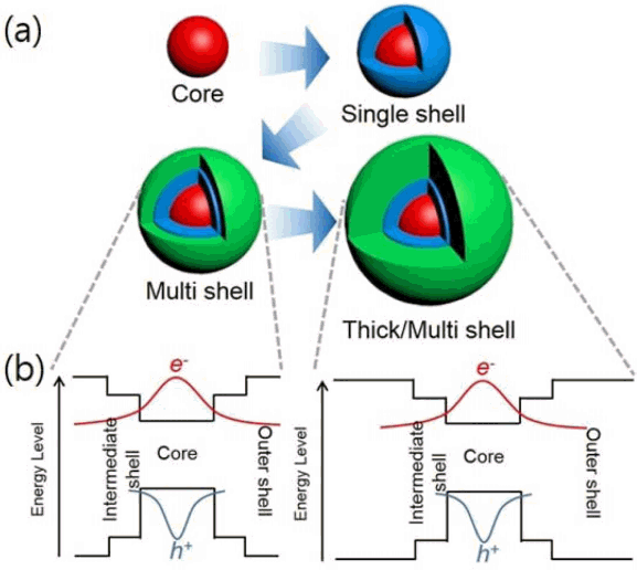
Schematics showing (a) evolution of core/shell QD structures and (b) energy level alignments and subsequent carrier localizations in multi- and thick/multi-shells.
The formation of a thicker outer shell is enabled by the presence of these intermediate shells; a thick shell plays a crucial role in enhancing the PL QY values and protects the core surface from surrounding mediums, decreasing the probability of surface degradation by light, oxygen, and water.44–48) In addition, the thick shell prevents charges from being leaked to trap sites on the shell surface. As shown in Fig. 4(b), the electron wave function can reach the shell surface in a thin multi-shell structure, but not when a thick shell is present; this phenomenon enhances the PL efficiency of QDs with thicker shells.49,50)
The organic ligands attached to the shell surface are important for determining the surface characteristics of the QDs. Generally, the head groups of the ligands are anchored to the surface of the QDs, and their tails are directed into the surrounding medium. Since the surface sites where the ligands are attached are the surface dangling bonds or defects, the PL properties and stability of the QDs are enhanced by the surface passivation provided by the ligands.51) In addition, the type of functional group determines which type of solution the QDs can be dispersed in; this is important for solution processing of the QDs.52) In addition, by maintaining the interparticle spacing, the ligands contribute to preventing aggregation of the QDs in solution, leading to monodispersed and colloidal QDs.53) Typical ligands include trioctylphosphine (TOP),1,53) amines,5) thiols,21) carboxylic acids,45) and mercaptopropionic acid (MPA).51,53)
2.3. Cd-containing QDs
Cd-containing QDs have been the most extensively investigated QDs and exhibit outstanding properties such as high PL efficiency (up to 100%),46,54) narrow emission line-widths (< 30 nm), and high stability under aggressive environmental conditions. In addition, they can emit all colors in the visible spectrum, including red (R), green (G), and blue (B) and can also be made to emit in the ultraviolet (UV) and near-infrared (NIR) regions by varying the particle size and composition.1,2,5,11,55,56) Common compositions of Cd-based QDs can be binary systems (e.g., CdSe,42) CdTe,56) and CdS57)), ternary systems (e.g., CdZnS,54) CdZnSe,58) and CdSeS1)), or quaternary systems (e.g., CdZnSeS24)). Cd-containing QDs have been used as fluorescent materials in LEDs due to their aforementioned advantages, which are the result of many studies to enhance their properties. Hence, in this Section, we discuss the characteristics of the Cd-based QDs with various core/shell architectures, in particular focusing on the type I structure for LED applications.
Enhancements of the optical properties and stability of CdSe QDs have been reported ever since CdSe QDs capped with ZnS were first announced.59) To improve the quality of the QDs to a level suitable for LED applications, a multishell system has been adopted. As mentioned previously, a key feature of this system is the use of a buffer layer to relieve the lattice mismatch between the core and the shell. Hence, in initial studies, a thin layer of either CdS or ZnSe was deposited between the CdSe and ZnS layers;42) however, lattice imperfections still existed. Next, alloyed and compositionally graded intermediate layers were used to further reduce this lattice strain; for example, CdSe/CdS/ZnxCd1-xS/ZnS QDs were developed by introducing an alloyed intermediate layer between the CdS and ZnS in the shell.43,60) In that study, the shell composition changed from CdS to ZnS in the radial direction, resulting from the forming of an alloyed ZnxCd1-xS layer by the successive ion layer adhesion and reaction (SILAR) technique. The particles showed a high crystallinity when analyzed by X-ray diffraction (XRD) and an improved PL QY of ~ 80% compared to that of CdSe/CdS/ZnS QDs (~ 50%).43) QDs synthesized using the same alloying process, but for the core rather than the shell, have also been developed.45,54,58) Alloyed ZnxCd1-xSe QDs were transformed from CdSe/ZnSe QDs by thermal treatment at high temperature, using the fact that group II cations diffuse more easily than the group VI anions in II–VI semiconductors.58) The researchers observed blue-shifted emission wavelength after alloying and increasing Zn content, as shown in Fig. 5(a). The QDs were much larger and had a higher crystallinity than the same color-emitting CdSe/ZnS QDs. Another approach for synthesizing compositionally graded QDs was presented by Bae et al.24) As shown in Fig. 5(b), using the difference in the reactivity of the precursors, they synthesized QDs with Cd- and Se-based cores and Zn-and S-based shells with a gradual change in chemical composition; the reactivities of the Cd and Se precursors were much higher than those of the Zn and S precursors. The QDs had a high luminescence QY of up to 80% and enhanced photostability.
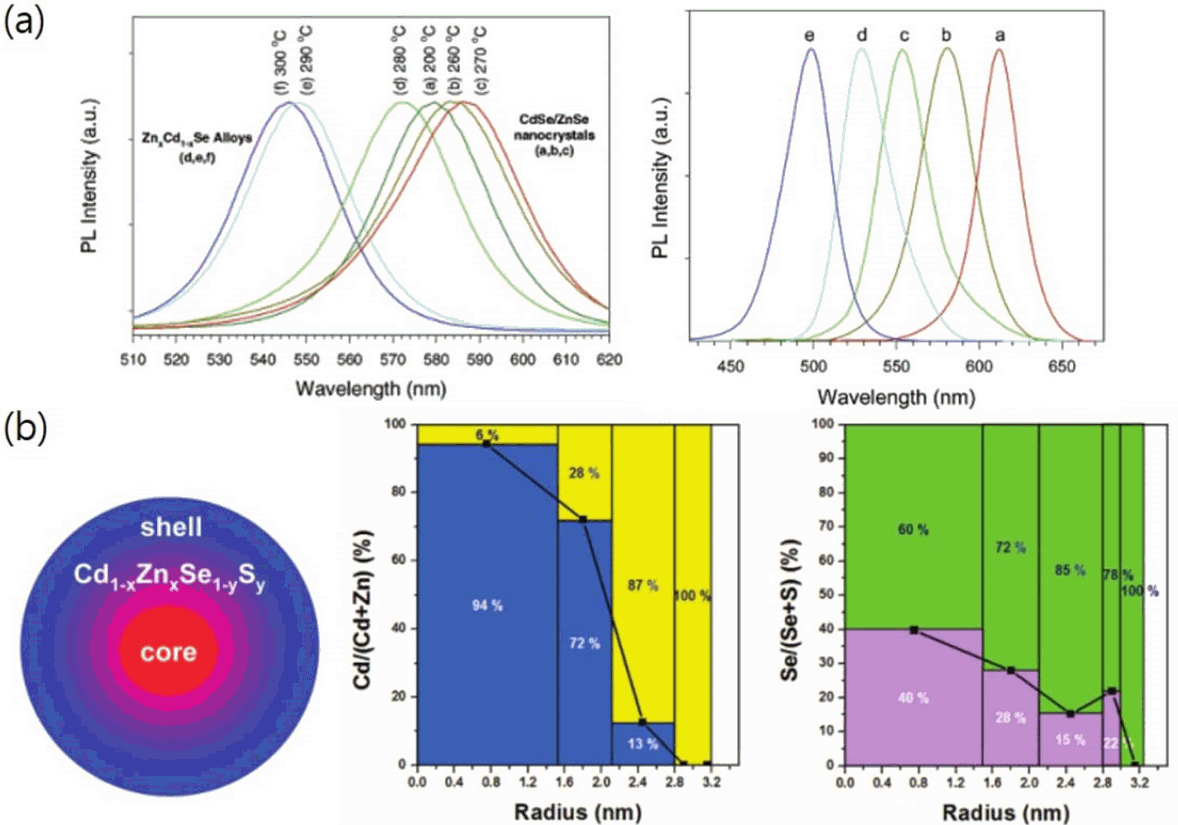
(a) Evolution of PL spectra in the progress of transforming CdSe/ZnSe core-shell QDs to ZnxCd1-xSe QDs under heat-treatment at different temperatures for 10 min each (left). PL spectra for ZnxCd1-xSe QDs with Zn mole fractions (x: 0, 0.28, 0.44, 0.55, 0.67 for a, b, c, d, e) (right). Reprinted with permission from ref. 58. Copyright 2003 American Chemical Society. (b) Schematic of the chemical composition within a QD (left). Ratio of Cd or Zn to (Cd+Zn) and that of Se or S to (Se+S) for each shell from the center of the QD. Relative values of each component (Cd, Zn, Se, and S) in each shell are shown (right). Reprinted with permission from ref. 24. Copyright 2008 American Chemical Society.
The development of the multi-shell system for Cd-based QDs led to an enhancement in their optical properties, which are suitable for practical application; however, there was a crucial issue regarding their fluorescence stability in degrading environmental conditions. Therefore, more stable QDs were developed by increasing the shell thickness. Jang et al. reported green emitting QDs consisting of alloyed core and thick multi-shell systems.46) Their CdSe@ZnS/CdSZnS QDs, with a size of about 7 – 9 nm and with a CdSZnS shell thickness of 1.3 – 2.5 nm, exhibited high fluorescence QY of 100% with enhanced photo- and chemical stability; the QDs retained 95% of their initial luminescence under UV exposure for 200 h. In addition, Yang’s group presented extremely large QDs with a thick ZnS outer shell; these QDs showed highly stable fluorescence properties.45,61) The blue-emitting QDs with an unprecedented size of 11.3 nm were composed of 6.1 nm diameter CdZnS alloy core and 2.6 nm additional ZnS outer shell (i.e., ~ 8.5 monolayers (MLs)), as shown in Fig. 6(a).45) Their PL QYs remained almost unchanged under different environments, which may generate surface trap sites due to detached surface ligands or surface oxidation, which can take place during ten-time purification cycles, 48 h UV irradiation, or ligand exchange processes (Fig. 6(b)). These improved stabilities were also observed for green-emitting 12.7 nm CdSe@ZnS/ZnS QDs with a 1.6 nm ZnS shell (i.e., ~ 5.2 MLs).61) The thick-shelled QDs, showing excellent stability, indicate a potential for outstanding performance in the LED applications.
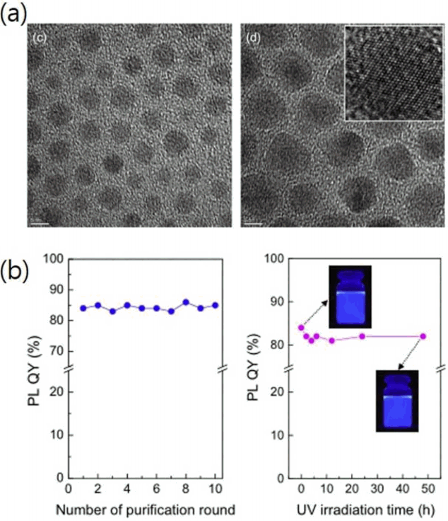
(a) High-magnification transmission electron microscopy (TEM) images of CdZnS (left) and CdZnS/ZnS QDs (right). (b) Changes in PL QY of CdZnS/ZnS QDs with repetition number of purification up to 10 rounds (left) and continuous exposure to UV irradiation (~1.4 W/cm2) for a prolonged period of time up to 48h. Fluorescent photographs of fresh and 48h-long UV irradiated QD dispersions with identical optical density are also compared in the inset of the right plot. Reprinted with permission from ref. 45. Copyright 2014 Elsevier.
2.4. Cd-free QDs
Although QDs containing cadmium show excellent performance, cadmium is a highly toxic element and its application has been limited by restrictions in many countries owing to its negative effect on the human body and environment. Therefore, practical applications using Cd-based QDs have been curbed. Hence, it is necessary to study materials for replacing the toxic QDs; a diverse range of candidates has been investigated. In general, the alternative QDs are InP20) in group III–V, CIS21) in group I-III-VI, and perovskite semiconductor nanocrystals.5) To date, the properties of these materials are still insufficient for practical applications and need to be improved to reach the level of Cd-based QDs. However, research into cadmium-free QDs is developing in a similar manner to that of Cd-containing QDs, and multi-, gradient-, and thick-shell systems are being investigated.
The III–V QDs are formed by combining Al, In, or Ga (group III cations) with P, As, or Sb (group V anions). Among these, the InP QDs, whose bulk band gap is 1.35 eV and exciton Bohr radius is about 10 nm,62) have been widely investigated for promising alternatives to Cd-containing QDs due to their tunable emission wavelength in the visible range. The properties of early InP QDs were quite inferior to those of Cd-based QDs and thus many studies to improve the fluorescence and stability of InP QDs with narrower emission line widths have been undertaken. InP QDs need to be coated with a shell of another material with a lower lattice mismatch, including ZnSe44,63–66) and GaP.20,67,68) As can be seen in Fig. 7(a), InP/ZnSe QDs possess a narrower FWHM compared to that of InP/ZnS; this is because the latter possess more interfacial defects due to their larger lattice mismatch (InP/ZnS: 7.7% versus InP/ZnSe: 3.2%), leading to more inhomogeneous PL broadening.63) Recently, Koh et al. presented InZnP QDs produced from either In-P or Zn-P intermediate complexes, which differed in growth kinetics each other.69) The presence of the Zn precursor in the initial stage of InZnP QD synthesis resulted in the formation of a Zn-P complex with low reactivity, leading to slow growth of the QDs, giving rise to narrow size distribution and emission linewidth (Fig. 7(b)). To enhance the PL QY and the stability of the InP QDs, the core/thick multishell system was again introduced, similar to the case of the Cd-based QDs. Available buffer layers for deposition between InP and ZnS are the above-mentioned ZnSe and GaP layers. The InP QDs with compositionally graded ZnSeS shells exhibited high fluorescence efficiencies of ~ 80% in both the red and green regions, improved photo-and chemical stabilities, and a larger particle size with a thicker shell compared to the InP/ZnS QDs.64,70) In addition, InP/GaP/ZnS QDs, which were synthesized by a heating-up process, were made to cover the full visible range by controlling the precursor ratio and the reaction time (Fig. 7(c)); resulting PL QYs values were 40, 85, and 60% and FWHM values were 51, 41, and 60 nm in the blue, green, and red regions, respectively.20) Very recently, Pietra et al. demonstrated more complicated core/multi-shell QDs of InZnP/InGaP/GaP/ZnSeS that exhibited excellent photostability under long-term LED irradiation of 5 weeks.68)

(a) Emission linewidth of InP/ZnS and InP/ZnSe using different indium halides and different precursor concentrations. Reprinted with permission from ref. 63. Copyright 2015 American Chemical Society. (b) Schematic description of the effects of metal–phosphorus complexes on the synthesis kinetics and color purity of In(Zn)P QDs. Reprinted with permission from ref. 69. Copyright 2017 American Chemical Society. (c) PL spectra of InP/GaP/ZnS QDs. Reprinted with permission from ref. 20. Copyright 2016 Nature Publishing Group.
For display applications, high-quality R-, G-, and B-emitters (primary colors) are important constituents. Both red and green emitters are expected to be obtained through further optimization of InP QDs. However, it is expected not to be possible to achieve blue emitters due to the relatively small band gap of bulk InP; the core size of InP QDs is extremely small to generate high-energy emission. It is difficult to produce sufficiently small cores during the nucleation and growth steps and, if achievable, the characteristics are expected to be unsatisfactory due to high surface defect density. Very few blue-emitting InP QDs have been presented to date, and their PL properties included emission wavelengths of > 475 nm and QYs of < 40%.20,71–74) ZnSe QDs have been explored as alternative blue-emitting, Cd-free QDs.75–82) ZnSe, one of the II–VI compounds, has a large bulk band gap of 2.7 eV, and can theoretically realize an emission wavelength of up to 460 nm with increasing particle size. To achieve high-quality ZnSe QDs with a type I core/shell structure, a simple ZnS or ZnSeS shell can be coated onto the ZnSe core in accordance with the band alignment requirements. Reported ZnSe/ZnS QDs, synthesized by various procedures including heating-up,78) hot-injection,80,81) and aqueous synthesis,82) showed fluorescence features with tunable PL emission in the range of 390 – 450 nm, narrow FWHMs of less than 20 nm, and fluorescence efficiency of up to 83%.81) However, their maximum PL QY was typically realized only at the short wavelengths of 420 – 430 nm, with the highest value of just about 68% at the PL peak wavelength of 450 nm suitable for display devices.
Due to their remarkable optical properties over the entire visible range, colloidal semiconductor nanocrystals, whose general formula is AMX3, and which have a perovskite structure (Fig. 8(a)), are newly emerging alternatives to Cd-containing QDs.5,83–89) Although it has been just a few years since colloidal perovskite nanomaterials were announced, they have demonstrated impressive PL performance: for example, high PL QYs of up to ~ 90% and high color purity (FWHMs of 12 – 40 nm). In the perovskite structure, the ability to emit light depends on the elements that occupy the A-, M-, and X-sites, where the compositions reported to date were organometal halide perovskites, CH3NH3PbX3,83) synthesized by the ligand-assisted reprecipitation method (LARP) at low temperature (owing to low thermal stability), and fully inorganic perovskites, CsPbX3,5) with improved thermal stability through substitution of Cs ions for CH3NH3 ions. Generally, the emission wavelength of the perovskite QDs can be controlled by varying the particle size or the composition of the X-site, which can be filled by the halide elements Cl, Br, or I (Fig. 8(b)). Unlike other QDs, the PL properties of perovskite QDs (e.g., QYs and FWHM) are not affected by dangling bonds on their surface.5) Although perovskite QDs have excellent PL characteristics for practical LED applications, there are critical problems related to poor stability and heavy-metal components. Their stabilities against high temperature, moisture, and light exposure are poor; they decompose or dissolve as polar water molecules interact with them. To solve this problem, various strategies, including a newly introduced surface capping agent84,85) or nanocomposite coating on the perovskite QDs,86) have been investigated. In addition, most perovskite QDs contain Pb, a heavy metal constrained for practical applications. Pb-free perovskite QDs, made by replacing Pb with either Sn87,88) or Mn,89) have been reported, but they exhibit very poor performance. Therefore, further studies to solve such obstacles are required in order to apply perovskite QDs to practical applications.

I-III-VI compound QDs have been also demonstrated as Cd-free technologies. There are many different compositions in the I-III-VI group, for instance, CIS,21) CuGaS2 (CGS),90) CuInGaS2 (CIGS),91) CuInZnS2 (CIZS),92) and AgInS2 (AIS).93) These materials are off-stoichiometric in cations (e.g., Cu, Ag, In, and Ga), generating cation vacancies or interstitial atoms. The defects produce defect states inside the band gaps and cause donor-acceptor pair (DAP) recombination, resulting in broad PL emission. The I-III-VI type QDs show high luminescence efficiencies of up to 85% for different wavelengths and tunable fluorescence covering the visible and NIR spectral regions, achieved by varying the ratio of the cations, by Ga2+ or Zn2+ alloying,91,92) or by replacement of S with Se94) (Fig. 9(a)). Studies on CIS/ZnS QDs have demonstrated that the ZnS coating led to dramatically enhanced PL QYs (from ~ 10% to ~78%);21) also, PL emission wavelengths of CGS-alloyed CIGS/ZnS QDs were blue-shifted with increasing amount of Ga2+.91) The recently reported Zn-Ag-In-S (ZAIS) QDs exhibited improved performance via the introduction of a Zn-In-S buffer layer in the ZAIS/ZnS QDs.95) As can be seen in Fig. 9(b), white PL emission covering the red to blue spectral region from a single CGS/ZnS QD was lately demonstrated; this emission originated from the spectral balance of two competitive intra-gap states, the conduction band-VCu and DAP.90) Due to these intrinsically broad emission line widths, high-quality I-III-VI QDs are appropriate for lighting applications, but not for displays.
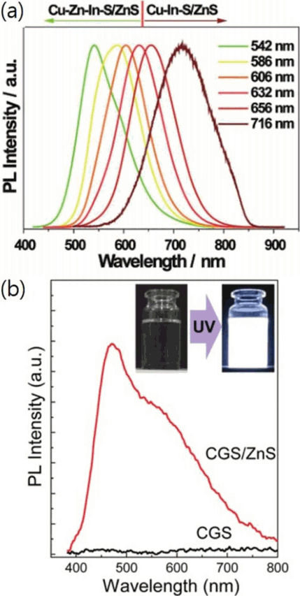
(a) PL spectra of as-prepared CIS-based emissive QDs. Reprinted with permission from ref. 92. Copyright 2012 John Wiley and Sons. (b) PL spectra of CGS core and CGS/ZnS core/shell QDs. Photographs of CGS/ZnS QD–chloroform dispersion without versus with UV irradiation are shown in the inset of (b). Reprinted with permission from ref. 90. Copyright 2016 The Royal Society of Chemistry.
3. Electrically Driven QLEDs
The emergence and development of QDs has had a great impact on various optoelectronic applications. In particular, taking advantage of the ability of QDs to emit colors over the entire visible spectral range, LEDs incorporating such technology have been seeing advances. There are two types of QDs used in LEDs for lighting sources. The first is the PL type,3,21,67) generally called quantum dot-based LEDs (QD-LEDs), which emit light after the absorption of photons from high-energy emitting near-UV or blue LEDs. The other is EL type, called QLEDs, which operate via radiative recombination of excitons formed by electrons and holes injected from the electrodes into the QDs. PL-type QD-LEDs have been developed with various structures such as edge-optic, enhancement film, and on-chip packaging; LCD TVs using this technology have been commercialized by many display manufacturers, including Samsung, TCL, Hisense, and Sony. Although the performance of these types of LCD TVs has been enhanced in comparison to those of classical LCD TVs, they have potential limitations relating to response time, viewing angle, contrast ratio, and design-freedom, all owing to the LCD frame. Hence, it is proposed that electrically driven QLEDs should be pursued as a next player to QD-LED. The following section discusses the operating principle of QLEDs, the factors affecting their performances, and their development status.
3.1. Operating mechanisms and structures of QLEDs
QLEDs follow an operating principle and structure similar to those of OLEDs. The basic structure of both devices consists of an anode, EML, and cathode. In this structure, electrons and holes are injected into the EML through the cathode and anode, respectively, and then form excitons and emit light via their radiative recombination. Therefore, to achieve highly bright and efficient devices, the charge carriers must be efficiently injected into the EML. To achieve this, multilayered structures have been investigated by inserting charge transport layers (CTLs), which are a hole injection layer (HIL), hole transport layer (HTL), and electron transport layer (ETL), between the electrodes and the EML, as shown in Fig. 10(a). As indicated in Fig. 10(b), by reducing the energy barriers between the electrodes and the QD EML, the presence of CTLs allows charges to be more easily injected (as shown by the energy band diagrams of the QLED with the standard structure).
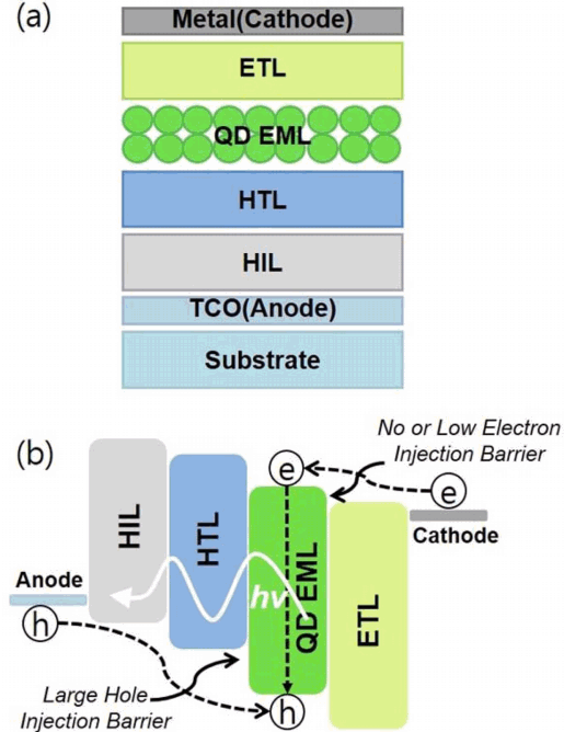
(a) Multilayered QLED device with a standard structure consisting of anode/HIL/HTL/QD EML/ETL/cathode and (b) corresponding energy level diagram.
When using an organic material as an HTL, to decrease the hole injection barrier, the highest occupied molecular orbital (HOMO) is located between the work function of the anode and the VBM of the QD EML. Owing to the large potential energy gap between the lowest unoccupied molecular orbital (LUMO) of the HTL and the CBM of the QDs, this layer also plays a significant role in blocking the leaking of electrons from the QD EML to the HTL under the influence of the electric field. The ETL, in a manner similar to that of the HTL, has energy levels that facilitate electron injection into the EML, while blocking holes from the EML. The multilayered structure, in which an EML is sandwiched between the HTL and the ETL having these energy band structures, enables the injected charge carriers to be confined in the EML, resulting in an increased probability of radiative exciton recombination. These conventional architectures consisting of anode/HIL/HTL/EML/ETL/cathode have been investigated by many research groups,1,14,54,55,61,64,71,79–81) and inverted structures, stacked between two electrodes in the reverse order of the standard ones, have also been developed.2,11,15,65,70,93)
The materials currently used in QLEDs have been well standardized, generally adopting polymer HIL and HTL materials and an inorganic ETL material. In 1994, the first reported QLED comprised an ITO anode, a poly(p-phenylenevinylene) (PPV) HTL, QD EML, and Mg cathode; device showed extremely low performance of < 0.01% EQE and luminance of ~ 100 cd/m.2,13) Later, devices employing either organic materials only55,96) or inorganic materials only as both HTL and ETL97) were demonstrated. The former devices displayed enhanced EL performance compared to previous ones, but were unstable when exposed to air and moisture. The latter devices had good device stability due to the nature of inorganic materials, but low luminance and efficiency due to damage to the underlying QD EMLs by the sputtering process used to deposit the oxide films. Hybrid QLEDs with a combination of both organic and inorganic CTLs exhibited dramatically improved device performance with respect to brightness and EQE;98) these types of hybrid devices have been continuously studied ever since.
3.2. Factors determining QLED performance
In QLEDs, there are various parameters used to evaluate the performances, for example luminance, power efficiency, and current efficiency (CE). However, these values depend on the color sensitivity of the human eye, which is sensitive to the colors in the order of green, red, and blue; as a result, it is difficult to compare absolute values at different wavelengths. To estimate the efficiency of different color emitting devices based on identical criteria, the value EQE has been used and is expressed as:
where IQE, ηoc, γ, and ηrad are the internal quantum efficiency, the ratio of the light out-coupling efficiency, the fraction of injected charges that form excitons (also called charge balance), and the radiative exciton recombination (also called emission efficiency), respectively. IQE is associated with γ and ηrad, and reveals how many photons are produced through the radiative recombination process of excitons formed in the QDs by the electrons and holes injected into the QD EML. The light out-coupling efficiency is related to the light confined or leaked in a device by refraction and reflection, originating from the difference between the refractive indices of the device components and air. Collectively, this equation means that EQE is the ratio of how many photons generated inside the device are extracted from it. Therefore, IQE and ηoc must be increased to achieve highly efficient QLEDs. The simplest way to increase IQE is to generate many photons in the QD EML. To achieve this, the non-radiative exciton decay processes occurring in QDs should be suppressed; QDs with core/shell structures are the best solution to inhibit exciton quenching processes.29) Many defects on the core surface of QDs result in intra-gap states which act as non-radiative decay centers. As mentioned in Section II-2, by coating the cores with shell materials, PL QYs are enhanced by core surface passivation which reduces the surface defects.26–28)
In core/shell QDs with high PL QYs and low surface defect densities, the primary non-radiative recombination mechanism under device operation is Auger recombination, a phenomenon in which the exciton energy is transferred to the extra electrons or holes in the charged QDs, resulting in the fluorescence quenching. A powerful strategy for minimizing Auger decay is to alter the abrupt confinement potential to a smooth one by using structural engineering to form an alloyed or compositionally graded intermediate layer at the core-shell interface (Fig. 11(a)).99–101) Bae and co-workers reported that QLEDs using two red-emitting CdSe/CdS QDs with or without a CdSexS1-x alloy layer, having similar optical properties and size, exhibited different EL performances.101) This difference was attributed to a favorable effect of the alloyed intermediate layer, arising from the suppression of Auger recombination. Controlling the shell thickness is another approach to mitigate the Auger process.35,102,103) In the case of CdSe/CdS QDs with quasi type II core/shell system, the electron-hole overlap is reduced with increasing shell thickness due to delocalization of the electron wave function over the entire core and shell regions.102)
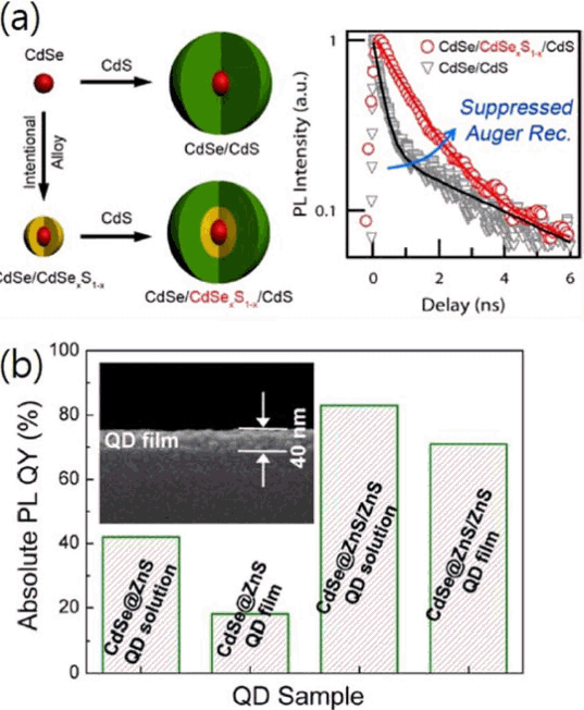
(a) Schematics of CdSe/CdS core/shell QD and CdSe/CdSexS1-x/CdS core/alloy layer/shell QD (left). Early time multiexciton decay dynamics in core/shell (gray triangles) and core/alloy layer/shell (red circles) samples. Reprinted with permission from ref. 100. Copyright 2013 American Chemical Society. (b) Comparison of PL QYs of CdSe@ZnS and CdSe@ZnS/ZnS QDs in the forms of solution versus solid film. Reprinted with permission from ref. 61. Copyright 2014 American Chemical Society.
The QD EML in QLEDs consist of closely packed multiple QD MLs. As the QDs of EML do not have perfectly the same size, the size distribution results in variation in their band gap. This causes efficient non-radiative Förster resonant energy transfer (FRET), whose rate sensitively depends on the distance (d) between QDs with a relation of ~ d−6, from the donor QD with a higher band gap to the acceptor QD with a smaller one. As the inter-QD distance increases, the FRET efficiency significantly decreases. Hence, large QDs with a thick shell are effective at suppressing FRET by increasing the distance between the cores of neighboring QDs.61,104) Yang et al. compared the QYs of CdSe@ZnS and CdSe@ZnS/ZnS QDs in solution versus film states.61) As shown in Fig. 11(b), the QY of CdSe@ZnS QD film was reduced by about 57% relative to that of the one in solution, while the value for the CdSe@ZnS/ZnS QD samples in film was found to be lower than that in solution (about 14%). These results reveal that the thick ZnS shell acts as an effective physical barrier, lowering the probability of a FRET event.
The most critical factor limiting QLED performance is unbalanced charge injection into QD EMLs from respective CTLs. The QDs, generally containing Cd, possess CBM and VBM positions at deeper energy levels compared to the LUMO and HOMO of organic HTLs, whereas the CBMs of QDs and inorganic ETLs possess similar energy levels. Hence, a large potential barrier for holes and a small one for electrons exist for charge injection into QD EMLs. In addition, the conductivities of ETLs are typically much higher than those of HTLs. As a consequence of combining these factors, electrons can easily migrate into the QD region, whereas holes cannot, resulting in the charged QDs that are a crucial factor determining the occurrence of non-radiative Auger recombination. In order to suppress Auger decay, many efforts to overcome imbalanced charge injection have been made by controlling hole or electron flows in the devices.14,105–108) The insufficient injection of holes relative to electrons in the QD EML can be mitigated by improving the mobility of HTL and/or by reducing the hole injection barrier at HTL/EML. Utilizing blended or bilayered structures with two types of HTLs, one of which provides a higher mobility or deeper HOMO level compared to the other, hole injection is facilitated.14) Meanwhile, insertion of an interfacial polymeric surface modifier (e.g., polyethylenimine ethoxylate (PEIE)) may enable a considerable reduction in the hole injection barrier at EML/HTL.105) Unlike the case of holes, dominant electrons in QDs are controlled by obstructing their flow. There are various methods for achieving this, including blocking excess electrons by introducing thin insulating layers between the QD EML and ETL,14,106) or using ETL materials to lower electron mobility.107,108) For instance, Mg-doped ZnO is an attractive material for controlling electron flow by widening the band gap and decreasing the electron mobility compared to those characteristics of ZnO. By replacing the ZnO ETL commonly used in QLEDs with ZnMgO, injected electrons can be better balanced with holes in the QDs. The use of Mg-doped ZnO ETL also suppresses the exciton quenching process, which involves exciton dissociation through a charge transfer process occurring at the interfaces between the QDs and ETL. In the case of ZnO ETL, the mid-gap states originating from oxygen vacancies are located at energy levels similar to those of the VBM of QDs and the holes in the QDs can be transferred to the adjacent ZnO ETL. However, the intragap defect states in ZnMgO are effectively reduced by Mg doping, and the interfacial charge transfer is suppressed. In addition, by employing doped metal oxide materials or inserting a thin additional layer at the interface of the QD and ETL, this exciton quenching process may be prevented.14,106–108)
3.3. QLEDs with Cd-based QDs
Most QD studies have focused on Cd-based materials; hence, electrically driven QLEDs using such materials have been the predominant focus of research. In 2011, utilizing crystalline ZnO nanoparticles (NPs) as an ETL, Qian et al. reported QLEDs based on fully solution-processed multilayer structures; the QLEDs showed excellent luminance values of 31000, 68000, and 4200 cd/m2 for R-, G-, and B-devices, respectively.98) Since then, most QLEDs have adopted identical ZnO NP ETL combined with different organic HTLs such as poly(N,N′-bis(4-butylphenyl)-N,N′-bis(phenyl)-benzidine) (Poly-TPD), poly(9-vinylcarbazole) (PVK), and poly[(9,9-dioctylfluorenyl-2,7-diyl)-co-(4,4′-(N-(4-sec-butylphenyl))diphenylamine)] (TFB). Relying on this multilayered architecture and further modifying the QD material and device structure, device performance has progressed steadily. Bright and efficient QLEDs consisting of ITO/poly(ethylenedioxythiophene):polystyrene sulfonate (PEDOT:PSS)/PVK/QDs/ZnO NPs/Al exhibited peak CEs of 46.5 and 2.2 cd/A and peak EQEs of 12.6 and 7.1% using blue CdZnS/ZnS104) and green CdSe@ZnS/ZnS QDs,61) respectively. These results were achieved primarily by using QDs with alloyed cores and thick shells to suppress non-radiative Auger recombination and inter-QD FRET. Later, Nanophotonica Inc. demonstrated that both the composition of the intermediate shell and the thickness of the outer shell in Cd1-xZnxSe1-ySy QDs are critical to the performance of QLEDs with respect to the efficiencies of charge injection, transport, and radiative exciton recombination.109) They synthesized QDs with fine nanostructures containing a ZnSe-rich intermediate shell, which effectively confined the excitons to the CdSe-rich core compared to the CdS-rich intermediate shell and the thin ZnS-rich outer shell. QLEDs using these QDs displayed high EQEs and CEs of 12% and 15 cd/A, 14.5% and 63 cd/A, and 10.7% and 4.4 cd/A for R-, G-, and B-devices, respectively (Fig. 12(a)). The surface ligands of QDs also play an important role in injecting charges into QDs during the operation of QLEDs, as they act as insulating layers that block charge injection. Replacing oleic acid ligands with shorter ones, 1-octaenthiol for blue QDs110) and tris(mercaptomethyl)nonane (TMMN) for green QDs,111) Li et al. produced QLEDs with high EQEs of 12.2% and 16.5% for B- and G-devices, respectively. Dai et al. improved QLED performance by optimizing the device engineering rather than the QD structures.14) As shown in Fig. 12(b), a QLED reaching the theoretical maximum EQE of 20%, assuming ηoc = 20%, and with a low efficiency roll-off, was developed. This was realized by promoting charge balance through facilitating hole injection by bilayered HTL, consisting of poly-TPD and PVK, and blocking excess electrons through introduction of an ultrathin poly(methyl methacrylate) (PMMA) layer between the red-emitting CdSe/CdS QD EML and the ZnO ETL.
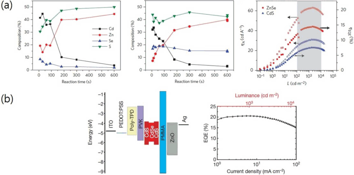
(a) Composition evolution of CdS-rich (left) and ZnSe-rich (middle) Cd1-xZnxSe1-ySy QDs. CE and EQE as a function of luminance for green QLEDs based on CdS-rich (blue triangles) or ZnSe-rich (red squares) intermediate shells (right). Reprinted with permission from ref. 109. Copyright 2015 Nature Publishing Group. (b) Band energy level diagram (left) and EQE versus current density and luminance (right) for the red QLED. Reprinted with permission from ref. 14. Copyright 2014 Nature Publishing Group.
QLEDs with an inverted device structure, in which various conventional organic materials with proven performances can be employed as HTLs by thermal evaporation, were first reported in 2012.2) Later, R-QLEDs manufactured by Mashford et al. exhibited a high EQE of 18%, enabled by an optimal charge balance achieved by controlling the distance between the exciton recombination zone in the QD film and the interface of the QD EML/ZnO ETL.112) These inverted-structure QLEDs cannot be fully solution processed due to destructive interlayer mixing between the QD EML and the solution-processed organic HTL. Recently, Kim et al. demonstrated an all solution-processed inverted QLED that overcame this problem by inserting an interfacial layer between the QD EML and the HTL.105) This device was composed of layers of ITO/ZnO NP/QDs/PEIE/Poly-TPD/MoOx/Al, in which the introduction of a PEIE layer prevented interlayer mixing and also enhanced hole flow by reducing the hole injection barrier by energetically upshifting the QD band levels (Fig. 13(a)). The efficiencies of this device were 65.3 cd/A in CE and 15.6% in EQE. Another approach to avoid damaging the underlying QD layer was explored; Zhang et al. used a deposition technique with a chlorobenzene solvent that caused no interlayer mixing.15) They produced inverted QLEDs with the tandem structure shown in Fig. 13(b). With optimized fabrication conditions, this G-QLED displayed the highest values of EQE (23.68%) and CE (101 cd/A) reported to date; however, this structure had the disadvantages of high turn-on and driving voltages owing to its overall increased device thickness.
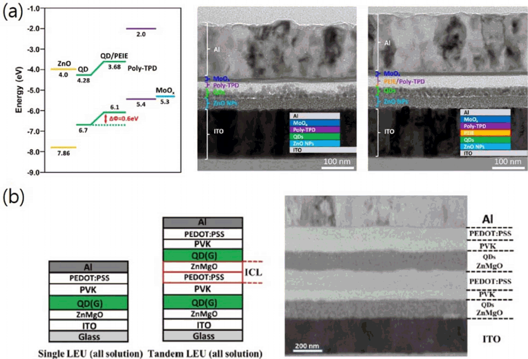
(a) Proposed energy band diagram of inverted multilayered QLED showing a VBM upshift of QDs by 0.6 eV when a 15.5 nm-thick PEIE was applied (left). Cross-sectional TEM images of all-solution-processed inverted device without PEIE interlayer (middle) and device with PEIE interlayer (right). Reprinted with permission from ref. 105. Copyright 2017 American Chemical Society. (b) Schematic device structure of all-solution-processed single QLEDs and tandem QLEDs (left). Cross-sectional TEM image of all-solution-processed inverted tandem QLED (right). Reprinted with permission from ref. 15. Copyright 2017 John Wiley and Sons.
Whereas most QLED work so far has been dedicated to the fabrication of monochromatic R-, G-, and B-devices, white and/or full-color-capable QLEDs, which comprise the QDs of multiple colors, have rarely been investigated. An earlier work discussed the interaction between QDs with different band gaps by examining the EL characteristics of white QLEDs, using QD EMLs consisting of different color combinations such as a dichromatic device with blue and yellow, trichromatic device with blue, green, and red, and tetrachromatic device with blue, cyan, yellow, and red.113) Later, Yang’s group demonstrated highly efficient and color-reproducible QLEDs based on an RGB QD-mixed layer.1) They analyzed the PL decay dynamics of the mixed RGB QD film and the relative EL spectral ratios of bichromatic and trichromatic QLEDs with different QD combinations, and proposed that, owing to an electric field-assisted inter-QD charge migration from the smaller band gap materials to the larger band gap ones, the red QD acted as a hole transport particle in the RGB QD-mixed EML. In addition, the white QLED possessed an excellent color gamut (as high as 126%) relative to the National Television Systems Committee (NTSC) triangle standard, a high brightness of 23352 cd/m2, and a high EQE of 10.9%.
3.4. Non-Cd QD QLEDs for display application
Among the non-Cd compositions described in Section II-4, appropriate QD materials for display applications include InP, ZnSe, and perovskite QDs; these materials have optical properties compatible with the primary RGB colors in the display, high PL QYs and, particularly, narrow emission bandwidths. Using red-emitting InP/ZnS QDs, the first reported InP QLED showed poor performance and impure color emission; white emission was observed, which was a mixture of red emission from the QDs and blue-green emission from the organic poly-TPD HTL.71) Later, Lim et al. used green InP@ZnSeS QDs with a compositionally graded shell and thin conjugated polyelectrolyte layer of poly[9,9-bis(3′-(N,N-dimethylamino)propyl)-2,7-fluorene]-alt-2,7-(9,9-ioctyl-fluorene) (PFN) in an inverted InP QLED.70) As presented in Fig. 14(a), InP QDs have higher CBM and VBM energy levels compared to those of Cd-based QDs, so InP QLEDs utilizing CTLs materials in Cd-based QLEDs experience charge carrier imbalance due to insufficient electron injection into the QDs. By enhancing the charge balance by inserting a PFN layer to lower the electron injection barrier between the ETL and QD EML, this InP G-QLED exhibited high EL performance of 3.46% in EQE and 3900 cd/m2 in luminance. In InP QLEDs, the effects of CTL materials on the device performance were examined. For example, two comparative HTLs of PVK and TFB were attempted64) and ZnO and ZnMgO were compared as ETLs.65) In the former case, with high-efficiency red InP/ZnSeS/ZnS QDs, the standard device structure consisted of ITO/PEDOT:PSS/HTL/multi-shell InP QDs/ZnO/Al, using either PVK or TFB as the HTL.64) Compared to the PVK-based QLED, the QLED using TFB had a higher mobility, resulting in a higher CE of 4.2 cd/A and EQE of 2.5%; however, TFB-derived parasitic EL emission was observed due to the lower hole-blocking barrier originating from the relatively deep LUMO level of TFB. The latter study was performed using either ZnO or ZnMgO NPs as the ETL material in an inverted structure.65) By lowering the potential barrier between the ETL and EML, compared to that of the ZnO-based device the ZnMgO NP-based InP QLED improved EL performance, showing a brightness of over 10000 cd/m2, CE of 4.4 cd/A, and EQE of 1.5%.
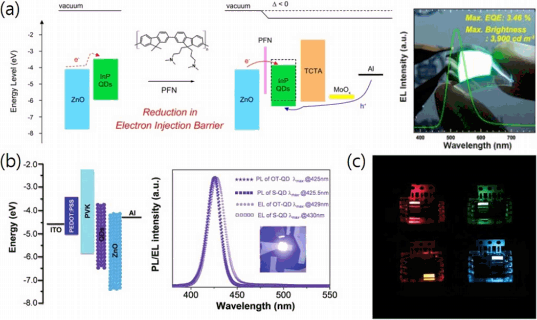
(a) Energy level diagrams of InP@ZnSeS QLEDs illustrating reduction in electron injection barrier between ZnO and QDs due to the presence of PFN layer (left). EL spectra of InP@ZnSeS QLEDs (right). Inset: Photograph of large-area and flexible InP@ZnSeS QLED. Reprinted with permission from ref. 70. Copyright 2013 American Chemical Society. (b) Energy level diagram of ZnSe QLED (left). PL spectra of ZnSe/ZnS core/shell QDs and corresponding EL spectra of violet QLEDs. Inset: EL image under an applied voltage of 11 V. Reprinted with permission from ref. 81. Copyright 2015 The Royal Society of Chemistry. (c) Images of perovskite QLEDs in operation. Reprinted with permission from ref. 118. Copyright 2016 John Wiley and Sons.
A few articles associated with ZnSe QLEDs with Cd-free blue or blue-like QDs have been published; however, the EL emission wavelengths have been in the violet-blue region of 420 – 440 nm.79–81,114,115) An earlier version of an ZnSe QLED using ZnSe QDs with a low PL QY of 40% at 420 nm showed a poor EQE of 0.65%.79) With more efficient ZnSe QDs, inverted ZnSe QLEDs were fabricated, displaying enhanced EL properties of 1170 cd/m2 in luminance and 0.51 cd/A in CE at an EL emission wavelength of 440 nm.114) Later, using high-quality ZnSe QDs and an optimized selection of CTL materials (i.e., PVK and ZnO) for good charge balance, highly efficient violet QLEDs were found to show a maximum luminance of 2632 cd/m2 and EQE of 7.83%. Although they had high efficiency, their emission color was near-violet, not suitable for display applications (Fig. 14(b)).81)
Perovskite QDs and their QLEDs have been significantly developed over a period of only a few years. There are two types of perovskite QDs, organometal halide perovskites (CH3NH3PbX3) and all-inorganic ones (CsPbX3); however, most perovskite QLEDs have focused on inorganic perovskite QDs. This is because organometal halide perovskite QLEDs still suffer from poor stability, spontaneous dissociation of excitons, and a high leakage current. Xing et al. introduced amorphous colloidal perovskite CH3NH3PbX3 NPs to suppress the exciton dissociation, and used them to manufacture green perovskite QLEDs that had a brightness of 3515 cd/m2 with an EQE of 3.8%.116) Compared to these devices, the inorganic perovskite QLEDs demonstrated better performance. The first reported inorganic perovskite QLED exhibited poor EL characteristics such as luminance values of 742, 946, and 528 cd/m2 and EQE values of 0.07, 0.12, and 0.09% for B-, G-, and yellow (Y)-devices, respectively.117) Later, more efforts were made to improve device efficiency by interface engineering of EMLs/CTLs118,119) or QD surface modification.120–123) Li et al. produced R-, orange (O)-, G-, and B-perovskite QLEDs by applying a trimethylaluminum (TMA) crosslinking method to the perovskite QD film (Fig. 14(c)).118) Their devices achieved EQE values of 5.7, 1.4, 0.19, and 0.0074%, respectively, enabled by efficient charge injection and a reduction of the leakage current. Recently, a high-efficiency inorganic perovskite QLED was presented, showing the highest EQE (8.73%) reported to date for perovskite QLEDs and a power efficiency of 31.7 lm/W.123) This result was attributed to the removal from the QDs, by an effective washing process, of excess ligands which act as an insulating layer. In addition, the tuned energy levels of PEDOT:PSS in the HIL played a crucial role in facilitating hole injection.
3.5. QLEDs with broad emission bandwidth for lighting applications
As a lighting source, a white light should possess wide visible spectral coverage to ensure a high color rendering index. In this respect, the QDs with broad emission bandwidths are preferred emitters for the fabrication of QLED lighting devices. On that account, I-III-VI type QDs with a highly broad PL character due to their intragap radiative recombination (as described in Section II-4) can be regarded as the most suitable QD emitters for lighting devices.92,124–130) Like many early versions of QLEDs with various QD compositions, ones using I-III-VI QDs initially exhibited poor performances (luminance of 450 cd/m2 and EQE of 0.033% with HTL-derived EL emission).124) The QLEDs employing organic HTL and ETL materials showed improved performances of 1200 – 2100 cd/m2 in luminance and 0.5 – 0.9 cd/A in CE.92) Later, the EL performances of quaternary CI1-xGxS QLEDs with ITO/PEDOT:PSS/PVK/QDs/ZnO NPs/Al structure were investigated and found to be strongly dependent on the CBM positions of CIGS QDs with different In-to-Ga ratios.125) With increasing Ga content, the EL values of CIGS and CGS QLEDs decreased compared to those of the CIS device, which displayed a maximum luminance of 1673 cd/m2, CE of 4.15 cd/A, and EQE of 1.54%. This was due to the increasing potential barrier to electron injection with increasing ratio of Ga in the EMLs. Controlling the electron injection barrier by replacing ZnO NP with ZnMgO NP as ETL, a tendency of improved EL properties with increasing Mg content was observed (Fig. 15).126) In such CIS QLEDs, a maximum luminance of 2785 cd/m2 (Zn0.9Mg0.1O ETL) and maximum efficiencies of 5.75 cd/A and 2.2% (Zn0.95Mg0.05O ETL) were reported. Very recently, record high efficiencies of 7.3% in EQE and 18.2 cd/A in CE from another CIS QLED were achieved by using an alloyed thick shell CIS/ZnS QD to suppress Auger recombination and FRET.127) Although CIS QDs have so far been almost exclusively chosen for the fabrication of I-III-VI QLEDs, devices with other compositions such as CGS128) and AIZS129) have recently been demonstrated. Among them, a white QLED with a single CGS QD EML that emits a white light covering the entire visible wavelength range from 400 to 800 nm was realized, showing a high color rendering index of 83 – 88 and EQE of 1.9%.128)

Proposed energy band diagram of CIS/ZnS, CIGS/ZnS, and ZCIS/ZnS QLEDs with Zn1-xMgxO NP ETLs (top). Maximum values of luminance (middle) and efficiency (bottom) of CIS/ZnS, CIGS/ZnS, and ZCIS/ZnS QLEDs obtainable as a function of ZnMgO NP ETL. Reprinted with permission from ref. 126. Copyright 2014 American Chemical Society.
4. Summary and Outlook
Since their emergence, QDs have attracted significant attention from various fields due to their unique optoelectronic properties. To achieve high-quality fluorescent QDs, type I core/shell systems were introduced and their properties, such as PL QY, FWHM, and stability, have been improved, mostly by fine engineering of the core/shell heterostructure, which also plays crucial roles in determining QLED performance with respect to Auger recombination and inter-QD FRET. In QLED devices, the charge carrier balance is an important factor in enhancing performance. Using the modulation of potential barriers and the insertion of thin insulating layers to controlling the injection and flow of charges, the efficiency of QLEDs has been dramatically improved. As a result, Cd-based QLEDs exhibiting the theoretical maximum EQE of 20% were demonstrated for red and green emission. However, the use of Cd-containing QDs for practical applications has been constrained due to the toxicity of Cd, thus requiring investigation on the synthesis of non-Cd QDs with environmentally-benign compositions and the fabrication of their QLEDs.
There are a few issues that can be addressed regarding the potential commercialization of QLEDs. First, development of synthetic protocols for three primary color high-quality non-Cd QDs with fluorescent properties at a level equal to or better than those of Cd-based QDs should be undertaken. This will potentially result in the fabrication of Cd-free QLEDs with performances in luminance and efficiency similar to those of highly efficient Cd-based QLEDs. Second, device lifetime is a particularly important issue from a viewpoint of future commercialization. Securing of similar operational lifetimes for the R, G, and B components of the display is critical. Excellent operating lifetimes of red and green Cd-based QLEDs that satisfy the requirements for display applications have been reported.14,109,111) On the contrary, in the case of blue QLEDs, the lifetime as well as the efficiency are far below the levels of their green and red counterparts, primarily due to the deep-lying VBM of BQDs, which is detrimental to efficient hole flow across the device. Therefore, new HTL materials with deeper HOMO energy levels, together with better hole mobility compared to conventional materials, are required. Additionally, to reduce the potential energy barrier. the introduction of surface modifiers that can shift the energy levels of the QD or HTL may also be undertaken. Lastly, compared to other competitive displays, solution-processability of QLEDs is a unique feature in device processing. To maximize this advantage, appropriate solution-based deposition techniques such as jet-printing131) and transfer-printing132) have been developed. Hence, further extensive research and development efforts in the QLED field should be devoted to overcoming the abovementioned technological barriers and thus leading to future commercialization.
As a final note, because they are similar to OLEDs, QLEDs possess a high freedom of device design, a fascinating aspect for next-generation displays, enabling the development of flexible and transparent devices instead of rigid and opaque ones. The total thickness of QLEDs, excluding the anode and cathode, is typically less than 200 nm. Therefore, flexible and transparent devices can be realized simply by substituting a rigid glass substrate with a highly flexible polymeric film (e.g., polyethylene naphthalate (PEN), polyethylene terephthalate (PET), or polyimide (PI)) (Fig. 16(a))70,105,128,132) and by replacing an opaque metal electrode with a highly transparent one (e.g., Ag nanowire, ITO, or graphene) (Fig. 16(b)).133,134)
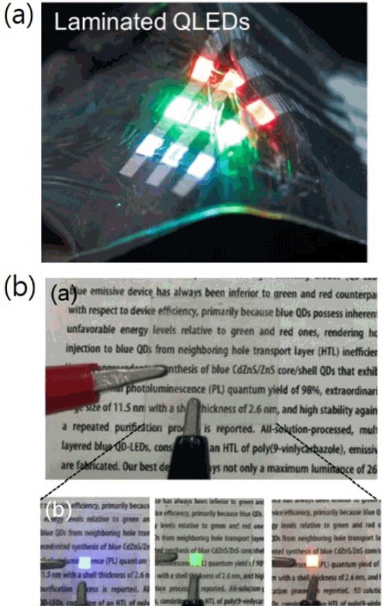
(a) Photograph of ultra-thin RGB QLEDs laminated on crumpled Al foil. Reprinted with permission from ref. 132. Copyright 2015 Nature Publishing Group. (b) Photograph of as-fabricated mono-colored QLED showing excellent visible transparency. Reprinted with permission from ref. 133. Copyright 2017 Elsevier.
Acknowledgments
This work was financially supported by a National Research Foundation of Korea (NRF) grant funded by the Ministry of Science, ICT & Future Planning (MSIP) (No. 2017R1A2B3008628); it was also supported by the Basic Science Research Program through the NRF, funded by Ministry of Education (No. 2015R1A6A1A03031833), and by the Korea Institute of Energy Technology Evaluation and Planning (KETEP) and the Ministry of Trade, Industry & Energy (MOTIE) (No. 20163030013980).