Effects of Mixing Ratio of Silicon Carbide Particles on the Etch Characteristics of Reaction-Bonded Silicon Carbide
Article information
Abstract
We prepared a number of reaction-bonded silicon carbides (RBSCs) made from various mixing ratios of raw SiC particles, and investigated their microstructure and etch characteristics by Reactive Ion Etch (RIE). Increasing the amount of 9.5 μm-SiC particles results in a microstructure with relatively coarser Si regions. On the other hand, increasing that of 2.6 μm-SiC particles produces much finer Si regions. The addition of more than 50 wt% of 2.6 μm-SiC particles, however, causes the microstructure to become partially coarse. We also evaluated their etching behaviors in terms of surface roughness (Ra), density and weight changes, and microstructure development by employing Confocal Laser Scanning Microscope (CLSM) and Scanning Electron Microscope (SEM) techniques. During the etching process of the prepared samples, we confirmed that the residual Si region was rapidly removed and formed pits isolating SiC particles as islands. This leads to more intensified ion field on the SiC islands, and causes physical corrosion on them. Increased addition of 2.6 μm-SiC particles produces finer residual Si region, and thus decreases the surface roughness (Ra.) as well as causing weight loss after etching process by following the above etching mechanism.
1. Introduction
Recently, line width of semiconductors has reduced to 10 nm, and microprocessing techniques are becoming more and more sophisticated. The top-down process for pattern forming technology includes Double Patterning Technology (DPT), Quadruple Patterning Technology (QPT), and Extreme Ultraviolet (EUV) technology. In actual practice, however, Self-aligned DPT (SaDPT) and Self-aligned QPT (SaQPT) are most preferred by using repeated sequences of Chemical Vapor Deposition (CVD), etch, and Chemical Mechanical Planarization (CMP). Compared to conventional processes, these newly-emerged technologies employ a CVD process instead of photolithograph for the formation of a sacrificial layer. Thus, they require a considerable number of etching and CMP processes for a fine pattern formation.
Especially, the etch process consists of DPT or QPT sequences, which are equivalent to three and five SPT (single patterning technology) processes, respectively. This leads to much longer exposure of various chamber components to the high powered and reactive plasma source.1) For the etch processes by DPT and QPT, therefore, the use of reaction-bonded silicon carbide (RBSC) has increased steadily to cope with the corrosion problem by applying plasma on Si-wafer supporters such as etch ring, focus ring, shield ring, etc.2,3)
It is well known that residual Si in the RBSC plays an important role on mechanical properties of the body. Its control, however, is not an easy task due to the interrelated complexity involved between pore size and distribution, ability of Si infiltration, formed green density, etc., which depend on mainly particle size of the starting raw materials.4–7) Thus, many studies have focused on the formed microstructure and mechanical properties in terms of raw materials, its particle size, and the amount of added carbon. However, the effects of residual Si in plasma etching have rarely been studied.7–10) Since green body microstructure decides the size and shape of residual Si in a reactionbonded body, it is believed that it also critically affects etcher part’s life and wafer’s rejection rate, especially during the etching process of semiconductors.
This study involves in the effects of mixing ratio of starting raw materials on microstructure development of residual Si in RBSC, and the corresponding RIE (reactive ion etching) behavior. We prepared RBSC samples with various mixing ratios by using four different sizes of SiC particles. Then, we evaluated the microstructure of the sintered bodies and their etching behavior.
2. Experimental Procedure
Starting raw materials include 95 μm, 33 μm, 7 μm, and 2.6 μm of SiC particles (> 99.3%, Showa Denko, Japan), Phenol resin (Phenol, KC-4100B, Kangnam Chemical Co. Ltd., Korea) as a binder and Si (Chunks, 99.99999%, Prime Grade, MEMC) as the infiltrating material. Table 1 shows the prepared batch compositions of various mixing ratios, which will be tested to identify the optimum microstructure with the minimal size of residual Si region.

Prepared SiC Samples with Different Mixing Ratios of SiC Particles
Figure 1 shows the flow of sample manufacturing and etching test for reaction-bonded body of SiC. First, 45 wt% of methyl alcohol and 5 wt% of phenol resin (based on dry weight of SiC particles) were mixed with SiC batch of predetermined mixing ratio in a mixer for 15 min. The mixed slurry were spray dried into granules (inlet temperature of 90°C, outlet temperature of 60°C, feed rpm of 16, disk rpm of 900). The prepared granules were cold-isostatically-pressed (Dr. CIP, Kobelco, Japan) for 5 min at 130 MPa into green body of ø100 × 300 mm.

Flow of experimental process.
Thermosetting phenol resin was carbonized in a dewaxing furnace by heating at a rate of 3°C/min and holding at 800°C for 5 h, which resulted in green body with many pores for easy Si infiltration. Dewaxed green bodies were stacked on a graphite felt in a vacuum furnace under a reduced pressure of 300 Torr, and heated at a rate of 3°C/min and held at 1,600°C in Ar atmosphere for 1 h for Si infiltration and subsequent reaction bonding. The reaction-sintered samples were machined into 10 × 10 × 1 mm, and mirror polished for microstructure observation under an optical microscope (Axio observer A1m, ZEISS, Germany) and an SEM (SUPRA55, ZEISS, Germany). The sintered apparent density was measured according to ASTM C20.
RIE test (SHE-4T-250R, Samhan Vac., Korea) was carried out under a dielectric etch condition with a flow of CF4 (30 sccm) +O2 (5 sccm) at 50 mTorr with power of 300 W and 13.56 MHz. Note that this test condition corresponds to more than 60% of total etching processes. Each sample was etched for 50 h and its weight reduction was measured with a precision balance (XB Series, CAS, Korea) and compared with each other. Etching behavior in terms of residual Si was also observed by analyzing the surface microstructure of each sample by CLSM (VK-X130K, Keyence, Japan) and SEM.
3. Results and Discussion
3.1 Microstructure and density of reaction-bonded body
Figure 2 shows images of optical microscopy on the prepared RBSC samples. It clearly indicates that gaps between coarse particles are filled with fine SiC grains forming a dense microstructure when the added amount of 2.6 μm-particle is increased from 10 to 50 wt%, while that of 9.5 μm-particle is decreased from 60 down to 20wt%. When the added amount of 2.6 μm-particle is 50 wt%, the residual Si region is fine and uniform as shown in Fig. 2(e).

Optical microscope images of RBSC specimens fabricated using different ratios of SiC powders (× 200): (a) DS1, (b) DS2, (c) DS3, (d) DS4, (e)DS5, (f) DS6.
When the addition of 2.6 μm-particle has increased to 60 wt%, however, the residual Si region becomes more fine, but part of it becomes irregular shaped with sizes of 20 ~ 80 μm as shown in Fig. 2(f). This observation contradicts the result by Park et al.,11) which reported pore sizes are normally in the range of 1/10 ~ 1/20 of the raw material size. This observation, however, is in agreement with the report by Shin et al.,12) which showed a similar gap shapes when gaps were densely packed. We then conclude that the most fine and uniform microstructure can be produced when 50wt% of 2.6 μm-particles fill gaps between coarse particles.
Figure 3 shows the density of each sample. In agreement with the above results of denser microstructure by increased fine particles, samples of Fig. 3(e) and (f) have an average density above 3.0 g/cm3. Samples of Fig. 3(a) and (b) with coarse microstructure, on the contrary, have an average density below 2.9g/cm3. Although Fig. 2(f) seems to be more dense compared to Fig. 2(e), its density as shown in Fig. 3 is slightly lower due to the nonuniform gap formation and irregular residual Si region. We conclude that denser microstructure can increase body density of RBSC only when the residual Si region is uniformly developed.

Variation of sintered density of RBSC specimens with different mixing ratios of SiC particles.
3.2 Change of surface roughness by CF4/O2 etching
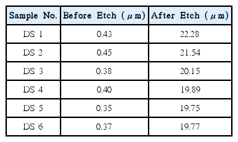
Figure 4 shows 3D surface images of RBSC samples after etching, and Table 2 summarizes the surface roughness changes before and after etching. Surface roughnesses (Ra.) of 0.35 ~ 0.45 μm before etching increase to 19.75 ~ 22.28 μm after etching. Even after due consideration of error in measuring surface roughness of differently-developed microstructure, the general trend is rather consistent.

3D micro-morphology of RBSC specimens with different mixing ratios of SiC particles: (a) DS1, (b) DS2, (c) DS3, (d) DS4, (e)DS5, (f) DS6.
Surface Roughness (Ra) of RBSC Fabricated Using Different Ratios of SiC Powders
The coarse-structured DS1 sample shows the highest Ra. number, as indicated as largely distributed red-colored parts in Fig. 4(a), that represent large surface unevenness. In the cases of DS2~DS6 samples, where 98 μm-coarse particles decrease and 2.6 μm-fine particles increase, surface roughness becomes gradually even in agreement with the trend of optical images in Fig. 2. This result implies that the fine particle addition is important to decrease residual Si region and to have a better surface morphology after etching in the RBSC body. Fig. 5 is weight loss data by etching for each sample, which indicates that a change of surface morphology eventually affected the etched amount.

Weight-loss curve of RBSC specimens after etching in CF4/O2 plasma at a bias power of 300 W with different mixing ratios of SiC particles.
Sample weights are in the range of 0.58~0.61 g before etching, probably due to the density difference by different mixing ratios of raw materials. After etching, however, we confirm that DS1 ~ DS3 samples show relatively higher weight losses, while DS4 ~ DS6 samples sintered to have a fine microstructure show relatively lower weight loss. Especially, the DS5 sample has the lowest weight decrease by etching.
Figure 6 is SEM images of two extreme samples, DS1 and DS5, after initial etching for one hour, which resulted in the largest weight decrease. In both DS1 and DS5 cases, we confirm that etching takes place firstly in the residual Si region. We believe that the etching mechanism involves two steps: The gases added, CF4 and O2, react and activate each other, forming COF2, CO, and CO2 gases and F and F2 radicals. Subsequently, free fluorine first attacks Si on sample surface to form SiFx for etching. It is known that Si has 3~4 times higher etching rate compared to SiC at room temperature.13–15)

SEM images of RBSC specimens after 1 h in CF4/O2 etching: (a) DS1, (b) DS5.
Figure 7 is microstructure of samples after 50 h etching. We confirm that the DS1 sample forms deep pits by preferential etching on the residual Si region, and coarse- and intermediate-sized SiC particles remain like islands. We observe a similar situation on the DS5 sample, but pits on the residual Si region are just under-cut shapes.

SEM images of RBSC specimens after 50 h in CF4/O2 etching: (a) DS1, (b) DS5.
Figure 7(a) shows the formation of coarse craters on the SiC surface, which is a typical phenomenon by corrosive ion bombardment. It implies that SiC corrodes rather physically by plasma-accelerated ions instead of by chemical corrosion considering the activation energy difference. Especially, the DS1 sample has much coarser craters compared to those of the DS5 sample due to more concentrated electric field on the island-shaped SiC as residual Si is progressively etched away by forming pits. We assume, therefore, field-activated ion bombardment along could accelerates physical corrosion and forms much coarser craters.
Thus the increase in etching time for DS1 ~ DS3 samples of more residual Si region could lead to increase in field non-uniformity and results in higher etching amount. With the mixing ratios of DS4~DS6 samples, it seems that low surface roughnesses (Ra.) are resulted from the evenly-developed microstructure during etching. We deduced that their finely-developed residual Si region generate finer pits in the corroded Si region, and their exposure to the relatively-uniform field distribution reduces the amount of etching.
4. Conclusions
In this study, we prepared RBSC samples with various mixing ratios by using four different sizes of SiC particles. We evaluated microstructures of the sintered bodies and their etching behavior in terms of mixing ratio of SiC particles, and conclude:
When the added amount of 2.6 μm-SiC was 50wt%, the sample showed the highest sintered density, and the residual Si region produced fine microstructure. When it had increased to 60wt%, however, the sample became slightly less dense, and the residual Si region became partly nonuniform.
After etching by CF4/O2 for 50 h, surface roughness (Ra.) of all sintered samples increased, and their weights decreased. The variations were relatively high for the DS1~DS3 samples with the coarse-microstructure of Si region, while they were relatively low for the DS4~DS6 samples with the fine-microstructure of Si region.
During etching process, the residual Si region was rapidly removed and formed pits isolating SiC particles as islands. This led to more intensified ion field on the SiC islands, and caused physical corrosion on them. Increased addition of 2.6 μm-SiC particles produced finer residual Si region, these changes were attributed to decrease at etched surface roughness (Ra.), as well as the weight loss decrease after etching process by following the above etching mechanism.