


1. Introduction
Impurity particle contamination has been considered to be one of the major technical issues in thin-film semiconductor fabrication via chemical vapor deposition (CVD). In general, it is known that over 50% of yield losses during the fabrication process can be attributed to micro-contamination. The damage of the semiconductor is particularly triggered by diffusing impurities such as sodium ions, metals, and particles into the interior of the semiconductor during the high-temperature process (thermal oxidation, diffusion, and epitaxial growth). Therefore, it is very essential to understand the transport phenomena of impurity particles in CVD reactors because the major source of contamination is the equipment.1,2) Impurity particles greatly affect the operation of devices and the formation of microstructural patterns. For example, impurity particles, which are generated from CVD reactors, lead to the formation of pinholes, voids, cracks, and defects, resulting in the breakdown of semiconductor devices.3-18) In the case of CVD reactors, the impurity particles, which lead to the contamination of semiconductor thin-films, mostly originate from the internal or external components of the reactors. The contamination is considered to be one of the major limitations of the otherwise efficient CVD process. For micro-electronic devices, as much as 75% of the yield loss can be attributed to impurity particle contamination of the wafer. It is known that there are two major sources of particle contamination: (1) cleanroom air, process gases, and people in the cleanroom, and (2) new particles formed inside the CVD reactor through chemical and physical processes. Because of the extensive effort to control the entry of particulates into the process, the first of these sources has largely been eliminated. At present, more than 80% of the total contaminant particles come from the chemical processing steps and mechanical movement of the equipment. In order to develop methods for controlling contaminant motions inside CVD reactors, it is first necessary to understand the impurity particle dynamics.
In this study, we have examined minimization of the number of impurity particles by replacing the load-lock chamber materials of the CVD equipment through optimization of the pumping method in the CVD chamber. Furthermore, a numerical simulation of the gas flow and particle dynamics in CVD reactors was performed that revealed the major influencing parameters and how the load-lock materials impact the substrate, which in turn provided the possible mechanisms for contaminant control.1)
2. Experimental Procedure
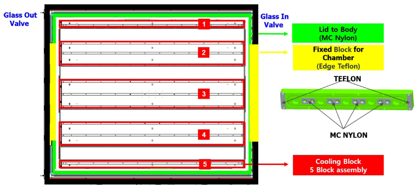
Generally, the number of particles tended to increase rapidly when the CVD system was down, and increased as the pumping speed increased. In our case, impurity particles were formed due to cracking of monomer casting nylon (MC nylon), which prevented metal contact between the chamber and cooling block. The impurity particles generated at the sites were analyzed by energy-dispersive X-ray spectroscopy (EDX). The indicated ingredient were carbon 66.7%, oxygen 9.6%, nitrogen 23.7% which was almost similar to that of each Blue MC nylon and White MC nylon Fig. 1 shows the area where the particles are generated. Table 1 shows the EDX data that compares the particles of MC nylon with the particles generated in the CVD chamber, bearing, and polishing solution. The MC nylon and CVD chamber particles are similar to each other.
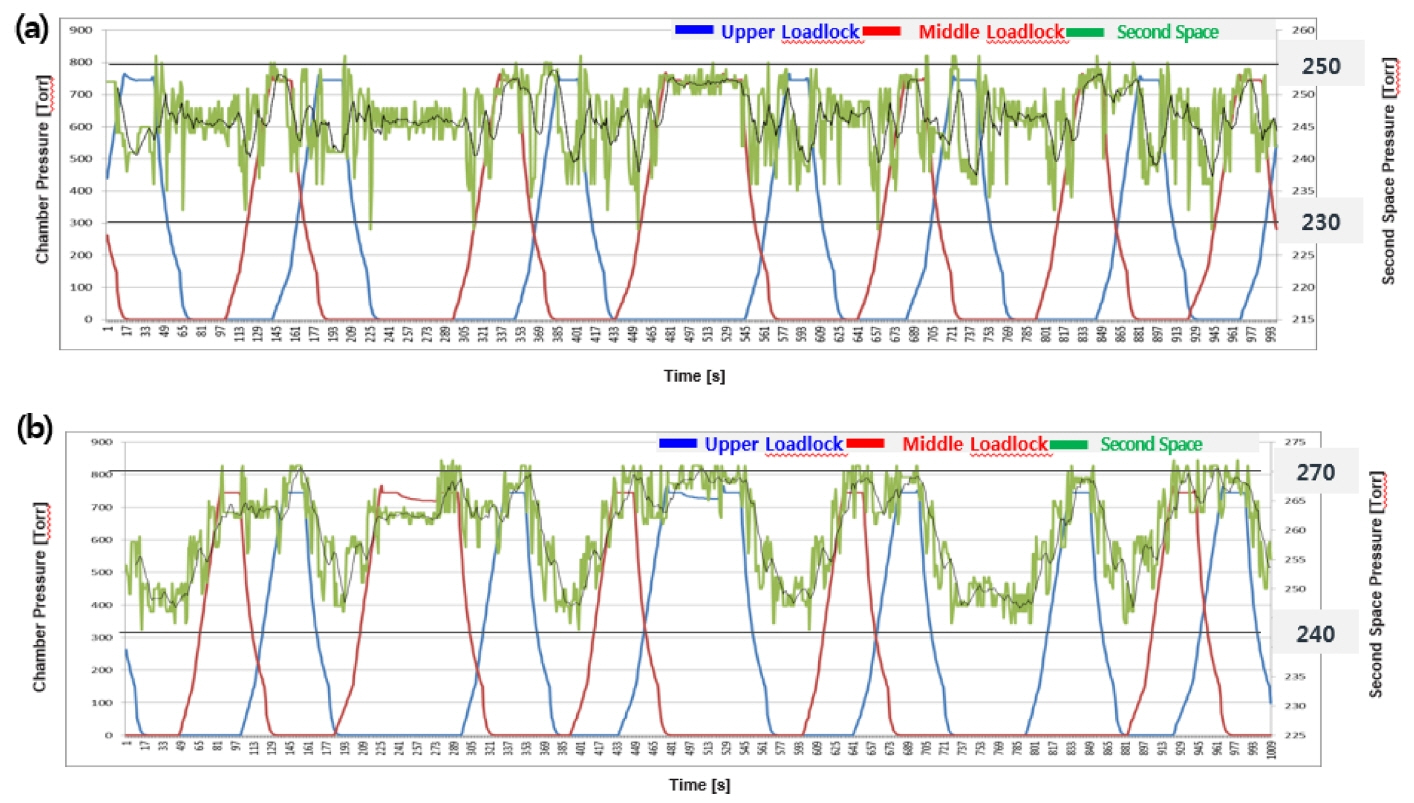
The following is a detailed description of the particle generation site. First, there is the ‘second space’, which is a sealed space between the upper chamber and the middle and lower chambers. A nitrogen outlet and pumping piping are installed. The second space is a space provided for buffering between the upper chamber and the lower lid. There is a lid between the upper and lower chambers of the equipment, which can be pumped to reduce the cracking of the chamber. The vacuum state of the upper chamber and the middle and lower chambers was confirmed for the leakage of the second space. As a result, the leakage of the second space caused particles to flow into the chamber. Fig. 2 shows the leakage test results of the second space. In the second space, it is a graph that confirms whether the pumping and vent is driven according to time. Fig. 2(a) shows the pumping and vent status of second space 1, whereas (b) shows the pumping and vent status of second space 2. This represents a graph that examines how much foreign matter flows into the chamber due to the leakage of the relevant part, and the pressure of the second space, which is the space between the lid and the chamber, changes. The Y-axis of the graph represents the pressure change in each chamber, and the X-axis represents time. As mentioned above, the CVD equipment consists of an upper chamber and middle and lower chambers, and the second space 1 shown in Fig. 2(a) is the space between the upper chamber and the middle chamber. As displayed in Fig. 2(a), in second space 1, the number of particles increases according to the difference in the pressure change. When the particle amount of the glass processed at the corresponding time zone was checked, it confirmed that the number of particles increased.
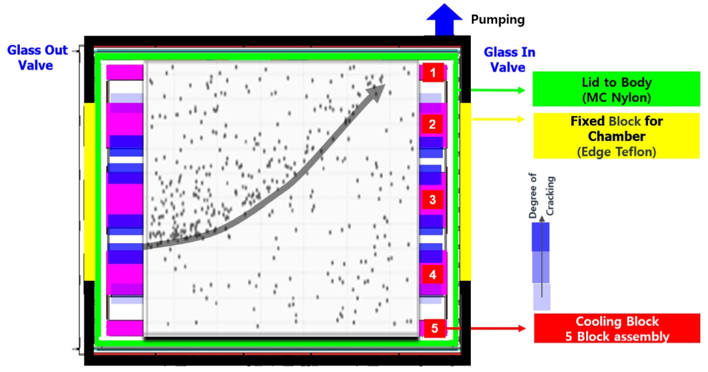
The second space 2 presented in Fig. 2(b) is the space between the middle chamber and the lower chamber. In second space 2, when the difference in the pressure change was high, we again confirmed that the particles generated by the MC nylon were introduced into the chamber. Other particle generation sites are the inside of the chamber and the outlet of the pumping port. As shown in Fig. 3, a facet block, cooling block, and lid portion are formed in the chamber. The particle map formed reveals linear behavior in the direction of the arrow along the exit direction of the pumping port outlet, as shown in Fig. 4. The point shown in the figure refers to each particle, and particle inspection equipment was used to check the particles on a 100 sheets of glass substrate and display the total number. By changing the angle of light (3-wavelength F\fluorescent) incidence, an operator can inspect the system. As shown in Fig. 4, particle generation and removal is possible through pumping control of the equipment.
3. Results and Discussion
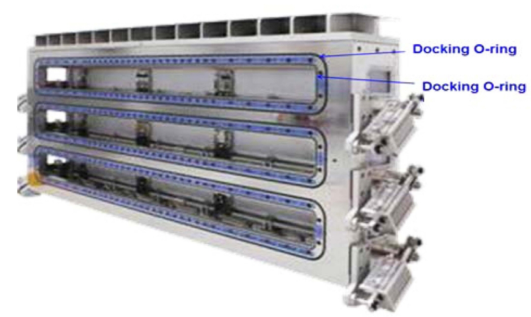
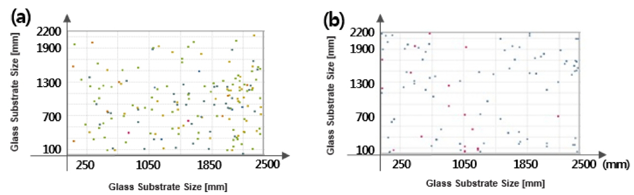
To solve the abovementioned problems, the following process and equipment improvements were carried out. In order to prevent the particles generated by cracking from entering the chamber by improving the equipment structure, the particle source was moved from the vacuum to the atmosphere region and the size of the O-ring was increased by a large amount (15%) to prevent its cracking As a result, it was confirmed that the amount of foreign matter was quantitatively reduced by 50% or more from 2.67% to 1.3%. Fig. 5 shows the effect of reducing the number of particles before and after the changing of the MC nylon position and the size of the O-ring. Fig. 5(a) shows the particle map before the MC nylon position and O-ring size were changed, whereas (b) shows the particle map after the improvement.
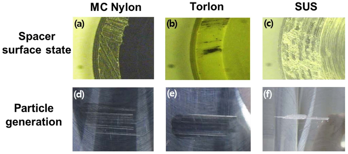
Furthermore, we changed the load-lock spacer material from MC nylon to Torlon. Torlon is superior than the other materials in terms of tensile strength, shear strength, hardness, coefficient of friction, rotation due to abrasion (limiting PV), and crack occurrence value by steel (wear factor), as shown in Table 2. Two tests were conducted to determine the extent of difference in particle generation due to the change in the load-lock spacer material. The first test imparted the same external vibration to each material, and the changes in the weight and surface state were observed. The upper and lower parts of the test specimen were wrapped with a urethane pad and subjected to vibration for 5, 10, 15, and 60 min with an air hammer. (Air hammer pressure: 0.07 MPa/2500 revolutions per minute of vibration/temperature: 20°C). As shown in Fig. 6, crack and particle generation were the least in Torlon.
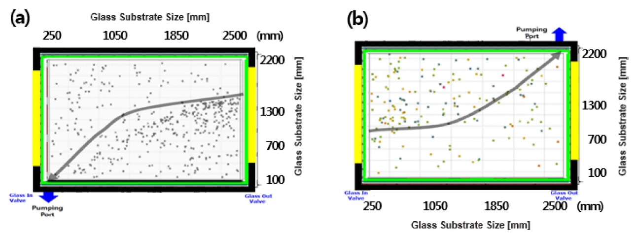
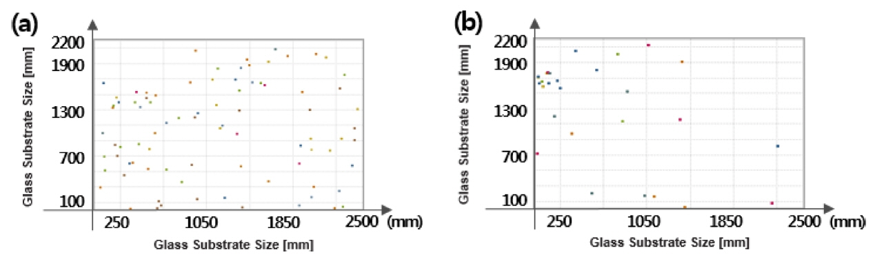
In the second test, the same friction was applied to each material, and the changes in the weight and surface state were observed. 500, 1000, 1500, and 2000 rubbings were applied by using a single-axis robot, and the changes in the weight and surface state were observed (distance: 30 mm, velocity: 24 mm/s). As shown in Fig. 7, crack and particle generation were the least in Torlon. Particles from the load-lock spacer material can enter the chamber and affect the pumping process. Fig. 8 compares the particle map generated by the pumping process involving the pumping port. Fig. 8(a) is the particle map of the glass in-port, and (b) is the particle map of the glass out-port. The color of each point on the map is different in order to distinguish whether the particle is an organic particle or a metallic particle.
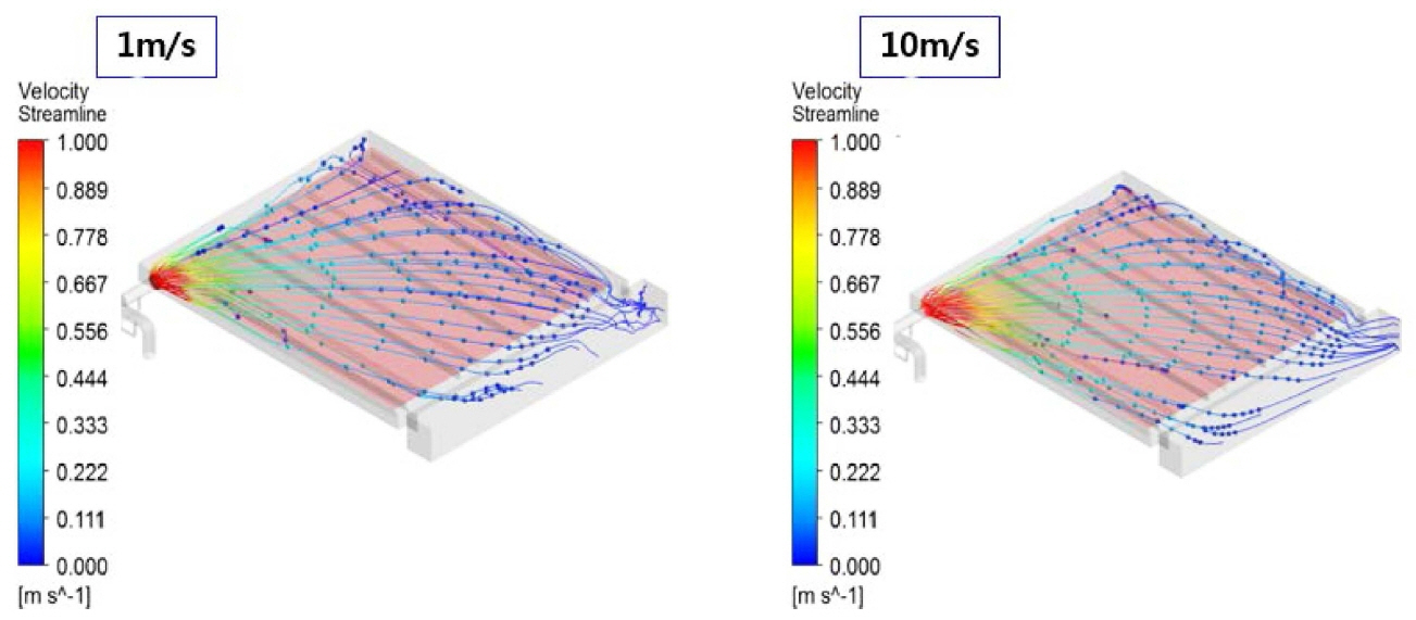
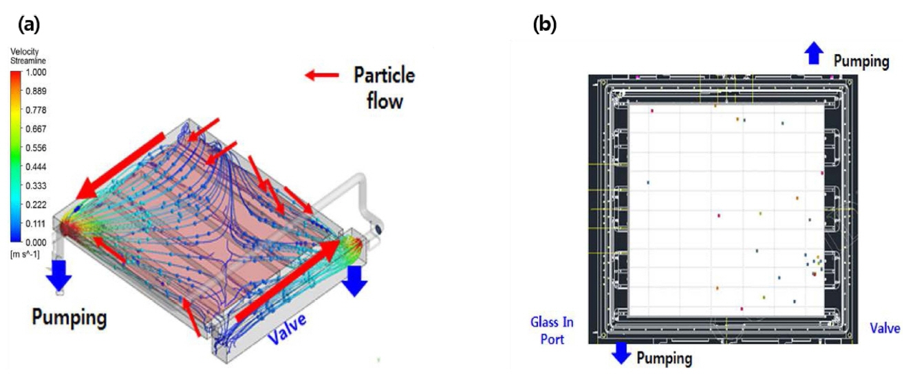
The faster the pumping velocity, the greater is the likelihood that the particles at the bottom will move upward. Fig. 9 compares the turbulence generated and the airflow developed airflow developed for pumping velocities of 1 and 10 m/s. Simulation results show that a high pumping speed is generated in the glass out valve, and repeated deformation is expected in the region 0.5 mm above and below the glass out valve docking area. It can be expected that the air flows generated in the pumping port part diagonally past the inside of the glass out valve during pumping. Regardless of the pumping velocity, the upper part of the glass has a higher flow velocity than the lower part and smooth flow is maintained.
ANSYS engineering simulation software was used for the pumping measurements, and the results are shown in Fig. 9; it is a useful system for measuring fluid movement direction and mobility during pumping. Fig. 8 shows the particle map formed by the pumping port, where it can be seen that a large number of particles remain in the portion not passing in the direction of the pumping arrow. The increase in the number of pumping ports will therefore lead to a reduction in the number of particles. Fig. 9 is a simulation of the air flow generated inside the chamber as a function of the pumping speed. It can explain the formation of the particle map shown in Fig. 8, apart from explaining the increase in the number of pumping ports and the control of pumping speed. We also understood how to adjust the position of the pumping ports to analyze particle flow and reduce particle size. Airflow is produced diagonally in the pumping port and turbulence is generated by the cooling block. The particle flow is also distributed in the direction of the air flow. Like the glass in the door port, air flows in the diagonal direction of the pumping port and turbulence occurs in the cooling block.
Figure 10 shows the air and particle flows inside the chamber when the pumping port is located at the dual port (glass indoor and glass outdoor). Unlike the previous two cases, it can be seen that air flow is generated at each part of the pumping port in the center part. There is almost no generation of particles, and a small number of particles are distributed at the edge, rather than at the center. In this way, particle generation was reduced from 2.67% to 0.52% by optimizing the pumping speed and appropriately placing the pumping port, as shown in Fig. 11. Fig. 11 (a) shows the particle map for single pumping and fast pumping situation, whereas (b) shows the particle map for dual pumping and slow pumping.
4. Conclusions
We examined the components of the particles that occur frequently in a CVD chamber and investigated ways to reduce them. In order to prevent the formation of particles, the particle source was moved from the vacuum to atmosphere area, the size of the part at the joint was increased, the type of plate of the docking blot was changed from the existing separate-type adapter-type, and the load-lock spacer material was changed from MC nylon to Torlon. In addition, during pumping, the pumping speed was decreased and the number of pumping ports increased to two to prevent the particles existing in the lower part of the chamber from rising. As a result, particle generation could be reduced from 2.67% to 0.52%. Through this research, it was possible to select the material of the part that can minimize particle generation during the CVD process and suggest a method to optimize the structure of the equipment.