


1. Introduction
Research on optical sensors utilizing nanomaterials has been actively conducted for numerous years; such optical sensors have been in the spotlight for their performance and efficiency. Also, various studies are being carried out on quantum dot technology, which uses size control to produce high quantum efficiency and convenient reproduction of a wide range of colors. Among such studies, research on photoconductive sensors has utilized conventional commercialized Cd and Pb, but these materials have problems including ingredient toxicity, high temperature process for synthesis, hazardous source materials, and high cost materials. Thus, ZnS quantum dots are in the process of commercialization because they are expected to adequately realize the role of photoconductive sensor due to their large band gap and stability under high currents. However, conventional Zn quantum dots require complex manufacturing processes and various types of equipment. Therefore, in this study, the room temperature solution method was applied to conveniently synthesize an ZnS:Mn2+ core and to establish a shell using ZnS. MPA was used as the precursor; the ZnS:Mn/ZnS quantum dot properties were observed according to the MPA content.
Moreover, photoconductive sensors of PN junction type and Schottky type were fabricated; the PN junction type sensor has the disadvantage of a complex fabrication process. On the other hand, compared to the PN junction type, the Schottky type allows for higher frequency usage and has a relatively simple fabrication process. Therefore, in this study, these characteristics were considered in the fabrication of a Schottky type quantum dot based photoconductive sensor; its performance as a sensor was investigated, as were the effects on the sensor of ZnS:Mn/ZnS quantum dots with various MPA content.1-6)
2. Experimental Procedure
2.1 ZnS:Mn2+ Quantum Dot Fabrication
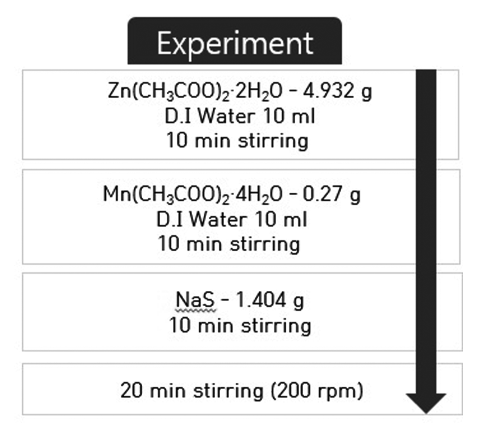
In this study, the wet reduction method, a type of chemical synthesis method, was used to synthesize ZnS:Mn2+ ZnS:Mn/ZnS quantum dots. First, the ZnS:Mn core was fabricated. Zn(CH3COO)2·2H2O (JUNSEI) and Mn(CH3COO)2·4H2O (DAEJUNG) were each dissolved in D.I water for approximately 10 minutes to prepare the aqueous solution. A specific amount of Na2S (ALDRICH) was added to the fabricated solution to form the ZnS:Mn2+ complex compound. Afterwards, the shell was formed. The fabricated ZnS:Mn core was dissolved in 200 ml of D.I water (see Fig. 1). For ZnS shell formation, after adding Zn(CH3COO)2·2H2O at a ratio of 0.1 relative to the core to the dissolved ZnS:Mn2+ core solution, MPA (3-Mercaptopropionic acid) was added in varying amounts. Then, after adding Na2S, the solution was dissolved for around 30 minutes at 200 rpm; this was followed by analysis of the final compound. In the case of MPA, the precursor formed, affecting the shell formation; the influence of the MPA content variation on the shell formation was analyzed.7-10)
XRD (Rigaku d-max/2200) was used to observe the synthesis and crystallinity of the final synthesized materials; PL Spectrum (FS-2) was measured to investigate the photoluminescence properties according to the MPA content. Also, the binding energy and band gap between the constitutive elements during the shell formation for each material were measured using XPS (PHI 5000 Versa Probe. Ulvac-PHI). TEM (FEI Co. Tecnai G2 F20) was used to investigate the particle size of the synthesized solution and the shell formation.
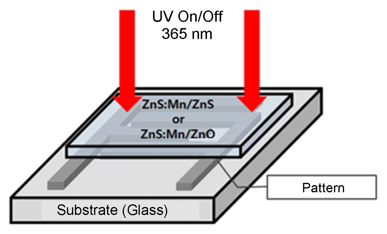
2.2. ZnS:Mn2+ UV Sensor Fabrication
For the UV sensor fabrication, lift-off photolithography with DFR (Dry Film Resist) applied on glass was used to form the Pt/Ti electrode pattern, with an electrode width of 100 um and a gap spacing of 100 um, as shown in Fig. 2. Afterwards, QDs with various MPA contents including 0 ml, 5 ml, 10 ml, and 15 ml in the ZnS:Mn core and ZnS:Mn/ZnS were applied. For the lift-off DFR pattern, an exposure amount of 180 mJ and development time of 4.7 min were used. For the electrode formation, considering the ZnS:Mn/ZnS QD properties, Pt was used because Pt exhibits low reactivity, does not react with nitric or sulfuric acid, and does not oxidize when exposed to oxygen. However, Pt has poor adhesion with glass, so the electrode was formed by deposition of Pt to a thickness of 100 Å after deposition of Ti to a thickness of 500 Å. Sputtering (DC magnetron sputter system) was used for Ti deposition at 200 W, 10 mtorr, and 6 sccm of Ar gas for approximately 10 min; this was followed by Pt deposition at 0.15 A, 10 mtorr, and 10 sccm of Ar gas for approximately 20 minutes.11-13)
The ZnS:Mn core, fabricated after the electrode formation, and the ZnS:Mn/ZnS QDs of various MPA content were applied to top of the glass. The solution was applied at regular amounts between 0.5 ml ~ 1 ml using a disposable pipette. After applying the solution, it was dried at room temperature and in a vacuum of 10−3 torr to prevent any impurities.
Since the fabricated sensor was supposed to react only with UV (365 nm), it was irradiated with Red (600 ~ 650 nm), Green (500 ~ 530 nm), Blue (450 nm), and UV (365 nm). A probe station (current probe) manufactured by TECH, which measured the current variation per material, was used to examine the potential of this device as a UV sensor.
3. Results and Discussion
3.1. XRD and TEM Analyses According to the MPA Content
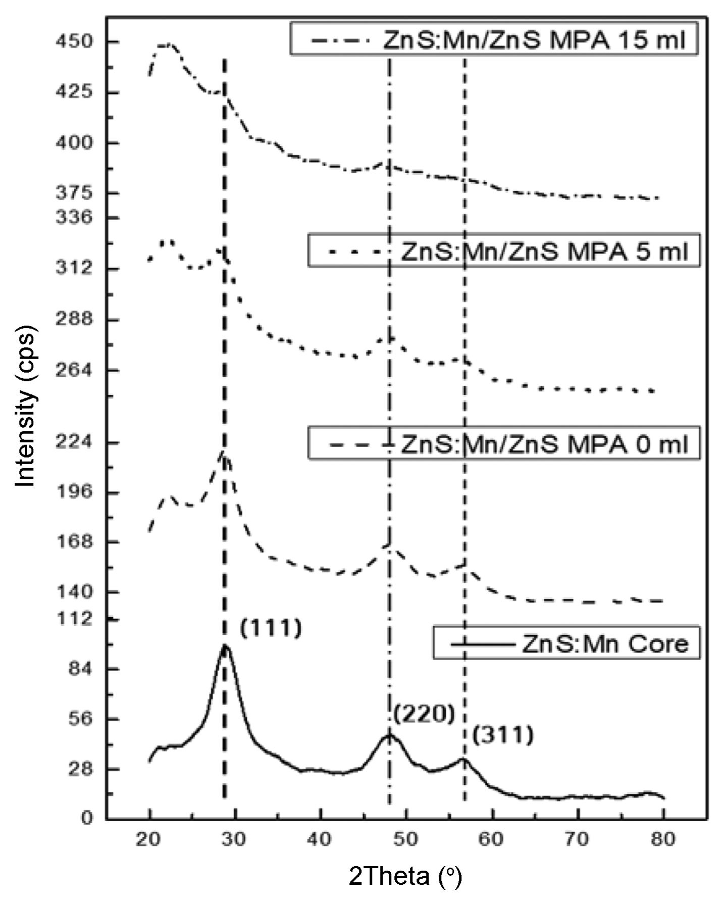
In order to investigate the phase change of the QD for each material according to the MPA content, which acts as the precursor, and according to the capping acid during QD formation, D/max-2200 XRD equipment manufactured by Rigaku was used to measure and analyze the X-ray diffraction pattern.
The liquid phase ZnS:Mn core and ZnS:Mn/Zns QDs were measured by using a pipette to drop approximately 1 ml samples of each on slide glasses and drying those samples at room temperature in a vacuum environment for 24 h.
In Fig. 3, the formation of a stable cubic structure of the synthesized ZnS:Mn core can be observed through the XRD diffraction pattern. As the MPA content increased, an increasing trend of the half-width of the ZnS shell peak was observed; this was due to the effect of increasing defects on the surface. It was thought that the half-width increased because of the failure to completely prevent the occurrence of defects on the MPA surface and the exhibition of amorphous characteristics of the MPA itself.
In order to determine the presence of shell formation for the fabricated QDs, TEM (Transmission Electron Microscopy) was conducted using the Tecnai G2 F20 model manufactured by FEI. For the TEM samples, particles were dispersed in D.I. water for 3 min using ultrasound; particles were then applied to a grid. Then, hot air drying was conducted at 80°C before the analysis. Measurement results revealed that the ZnS:Mn/ZnS shell had one layer form on the outermost exterior. In Fig. 4, it can be observed that the particles were of spherical shape and that the cores of the particles had a lattice structure of 3 Å, matching the lattice structure of ZnS:Mn, with crystalline formation. However, the ZnS portion of the outermost layer, which appeared to be a shell, was amorphous and its lattice structure unclear. Through this, the formation of the ZnS:Mn core-shell was observed.
3.2. PL Property According to the MPA Content
Photoluminescence (PL) variations of the core and synthesized QDs were measured to investigate the optical properties according to the MPA content during the ZnS:Mn2+ ZnS synthesis. The results were plotted and compared. The PL spectrum was measured using a quartz tube. According to the PL peak location on the graph shown in Fig. 5, it was determined that the ZnS:Mn2+ core was emitting orange light at 603 nm. In addition, absorption during the fabrication of ZnS:Mn/ZnS QDs was found to be between 290 nm to 300 nm, as shown in Fig. 5(a); the absorption spectra did not show significant differences depending on the MPA content. On the other hand, the emission spectrum showed that the PL peak location shifted from 603 nm to 598 nm with increasing MPA content, as shown in Fig. 5(b); as the MPA content increased, the PL intensity also significantly increased relative to that of the 0 ml MPA ZnS:Mn/ZnS sample. This result was due to the formation of a thiol ligand on the surface to facilitate the formation of the ZnS shell as more MPA is added to the ZnS:Mn core. As a result, the core-shell structure formation became more stable as the MPA content increased.
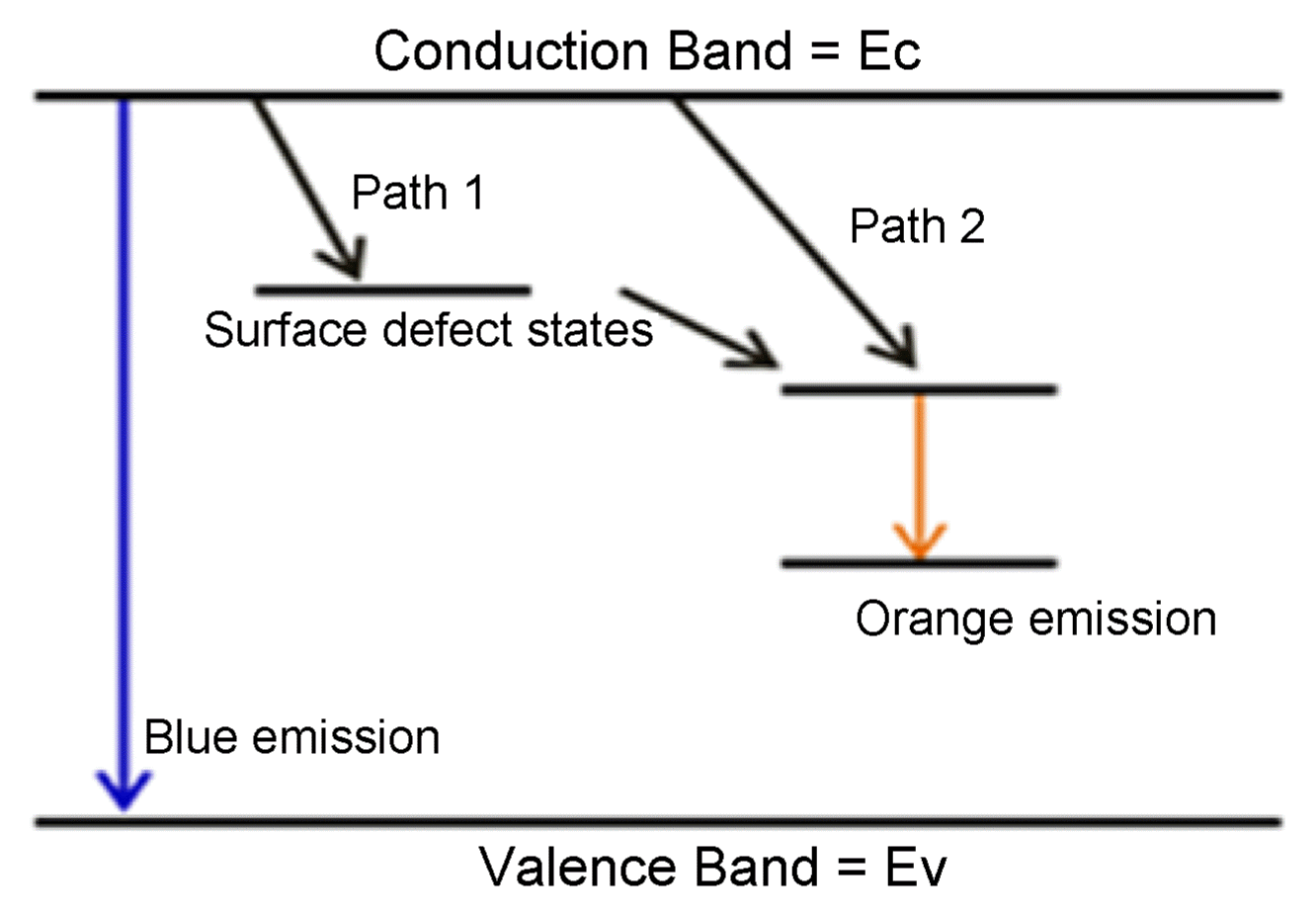
The PL intensity increase and peak shift can be explained using the quantum effect, in which electron movement, which was unrestricted in the core, is no longer unrestricted beyond the shell. Electron movement was now limited to within the core because of the formation of the core-shell structure; this results in quantum efficiency and PL intensity increase due to increases in electron movement. Also, MPA acts as a precursor during the core-shell formation; however, unsaturated bonding at the surface could not be completely prevented, and this produced defects on the surface. Such defects form a defect level between the valence and conduction bands and induce a phenomenon in which excited electrons do not move to the doped Mn2+ level and emit but rather move to the above defect level and then become excited (see Fig. 6). In this manner, either a PL peak shift from 603 nm to 598 nm or a blueshift was observed.14)
3.3. XPS Properties According to MPA Content
Table 1 shows the measurement data, obtained using XPS to calculate the Zn bond loss energy, for the fabricated ZnS:Mn2+ QD band gap during the ZnS shell process. The calculated results show that as the MPA content relative to the core increased, the ZnS:Mn/ZnS QD band gap increased.15) The same conditions were used for the core; the varying parameter was the MPA content. As such, it was deduced that the calculated band gap reflected the shell characteristics. This result was related to the PL intensity measured earlier. The ZnS shell QDs had a type 1 structure (Fig. 7), in which the core band gap was smaller than the shell band gap. In this case, core electrons and holes are not lost to the outside; instead, the electrons and holes exist within the core and are simultaneously delocalized due to the peak shift and defects.16-18) Therefore, electrons and holes exist within the same structure for type 1 structures, and this affects the PL intensity. Also, as the band gap increases, recombination of electrons and holes becomes easier, increasing the electron drought effect with regard to quantum efficiency. The probability of electron and hole recombination increases; this recombination causes the emission of radiative and nonradiative energy, which in turn increases the PL intensity.
Figure 8 shows the S binding energy according to the MPA content; it can be seen that the S binding energy increased as the MPA content increased. This result was thought to be due to changes caused by the ZnS shell formation. Compared to the S binding energy for core formation, the S binding energy for the 15 ml MPA ZnS:Mn/ZnS sample increased more than that for the 0ml MPA ZnS:Mn/ZnS; this result was due to the ZnS:Mn bond in the case of the core. As the MPA content increases, the binding energy variation for the ZnS shell formation changes, and the above results show that the formation was stronger with increased MPA content. This result is related to the band gap calculations carried out using the Zn bond. Considering the results of both increased band gap and strengthened S binding energy as the MPA content increased, it can be said that the electron drought effect of the QD core-shell increased with increasing MPA content, resulting in increased PL intensity.
3.4. UV Sensor R.G.B Test
Figure 9 shows the response and the current amount of the fabricated sensor when Red (600 ~ 650 nm), Green (500 ~ 530 nm), Blue (450 nm), and UV (365 nm) light were used to irradiate samples. The experimental method involved turning the UV and RGB on and off at 60 s intervals to check whether the sensor responded. Also, the response variation was investigated by continuing the on and off process at 60 s intervals for a total time of approximately 980 s. Through this, it was found that the fabricated sensor responded only to UV, with a current amount variation of around 2.19 × 10⁻¹³ A; the amount variation with respect to time was insignificant, at about 0.1%.
These results can also be verified using Eq. (1), in which the energies calculated for the wavelengths of Red, Green, and Blue do not exceed approximately 3 eV.
Red, Green, and Blue, which have low energy, did not have sufficient energy to excite the electrons within the band gap, so electron movement did not occur and the sensor did not respond. On the other hand, UV (365 nm) with an energy of 3.39 eV, excited the electrons and the sensor responded. When the UV was turned on, energy was transferred, causing electron movement and current change. When the UV was turned off, there was no response because of the lack of electron movement.
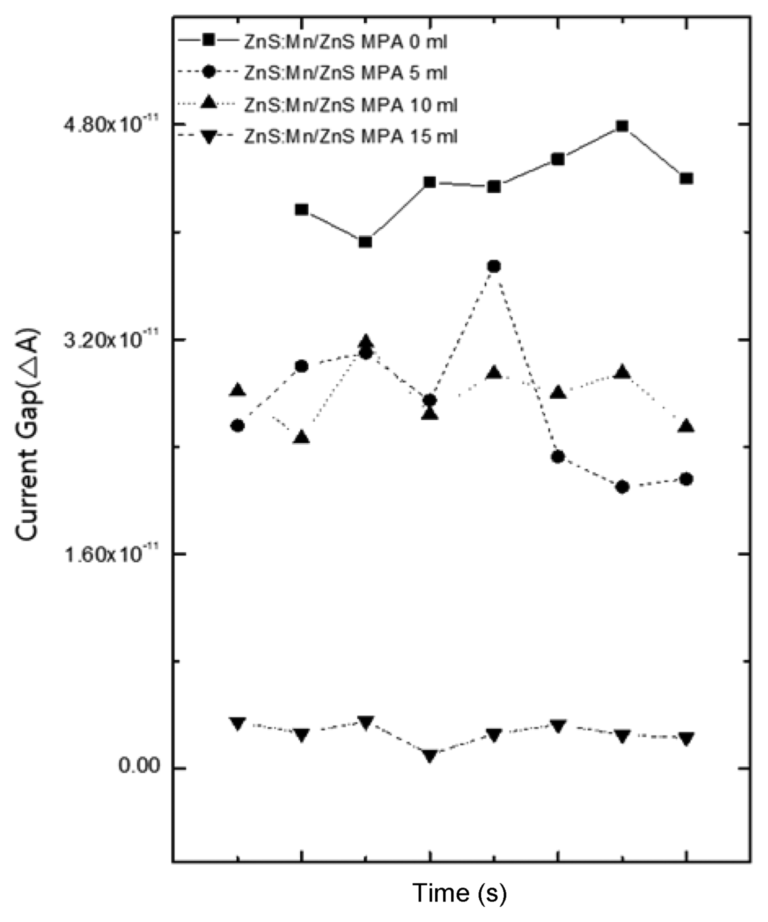
3.5. Sensor Response According to MPA Content
The sensor response according to the MPA content was investigated; the results are shown in Fig. 10. As the MPA content increased, the amplitude and current decreased. This result is related to the Schottky diode structure: the operation of the Schottky diode is affected by defects within the band gap as well as by the dangling bond in the interface and internal defects. Taking into consideration the XRD measurement result data, it was observed that surface defects increased with increasing MPA content during the ZnS:Mn/ZnS QD fabrication; such surface defects exist in the form of additional layered defects as the shell forms, so that the electrons captured by the electron drought effect are recaptured by a different defect layer, resulting in increased resistance and degraded sensor properties.19-21)
Also, based on the XPS data, the ZnS:Mn/ZnS QD band gap results revealed that the band gap increased as the MPA content increased; Fig. 10 shows that this result has an effect on the sensor as well. UV (365 nm), which provided the energy that drove the sensor, has relatively low energy. When such low energy is used to irradiate the sample, the band gap increases and the traps within the band gaps (defect level) exist in a layered form. In the case of QDs, the electrons do not receive sufficient energy to move from the valence band to the conduction band; the resistance increases as electron movement becomes difficult due to traps between the valence band and the conduction band. As a result, the sensor response variation range was almost 0 and the variation with respect to time was very small at around 0.1%.
Meanwhile, when the band gap is small, the layer defects produced due to MPA increase during shell formation also decreased and this allows for electron movement from the valence band to the conduction band with only small input energy. For the first 60 s, no response was observed; however, with time, the response variation increased to about 0.8%.
Thus, the ZnS:Mn/ZnS QD based sensor exhibited excellent sensor characteristics when the MPA content decreased.
4. Conclusions
The investigated properties of the ZnS:Mn2+ ZnS shell quantum dots fabricated using the room temperature solution method revealed that for ZnS:Mn/ZnS, the PL peak shifted from 603 nm to 598 nm and the crystallinity decreased as the MPA content increased; however, the PL intensity increased by about 613% for the 15 ml MPA sample, in contrast to that value of the 0 ml MPA sample, which saw no increase. Diffraction patterns showed that the ZnS shell half-width increased as the MPA content increased; this led to a decrease of the crystallinity. For the ZnS shell, it was observed that the band gap increased as the MPA content increased.
As for photoconductive sensors, their properties improve because the pattern electrodes are closer. R.G.B testing carried out to evaluate the potential of this material for use in a UV sensor showed that the energies calculated using the wavelengths for R.G.B did not exceed 3 eV, while the energy for UV was about 3.39 eV. Hence, the sensor was observed to respond when the wavelength energy was greater than 3 eV. Furthermore, for the ZnS:Mn/ZnS QDs, the maximum current (A) decreased from 4.00 × 10⁻¹¹ A to 2.62 × 10⁻¹² A as the MPA content increased; this was deduced as being due to the increase in the surface and internal defects, leading to these defects taking the form of layer defects. This result was attributed to the variation in the band gap, calculated from the XRD diffraction pattern and XPS results.
For the ZnS:Mn/ZnS QDs, the sensor characteristics were observed to degrade as the MPA content increased.