


1. Introduction
Dye-sensitive solar cell (DSSC)1) is low in production costs compared with the existing Si solar cells,2) and is transparent as well as capable of producing devices with various colors so that application in diverse areas is expected.3) However, whereas energy conversion efficiencies (ECEs) of the Si solar cells are about 20%,4) those of DSSC are relatively low at about 11%,5) requiring studies to solve this problem for commercialization.
Enhancing ECE of the DSSC involves in studying for all its components such as working electrode (WE), electrolyte, and counter electrode (CE). Especially, most focused one has been the WE that is composed of transparent conductive oxide (TCO) substrate as a conductive layer,6) blocking layer (BL, compact TiO2) to prevent electron recombination,7) semiconductor oxide layer (mesoporous TiO2) as an electron transport layer,8) and dye for forming electrons and holes upon receiving light.9)
Studies on the semiconductor oxide layer is most active among such components for the WE, and engineering of semiconductor oxide layers is being realized through structure modification, band gap conversion, and combination with other materials, etc. In the case of structure modification engineering, S. H. Lee et al.10) have prepared a TiO2 nanohelix structure as a physical vapor deposition (PVD) on fluorine doped tin oxide (FTO) substrate by using the glancing angle deposition method and reported an increase in ECEs by 6.20% in comparison with the existing 7.91% through the light harvesting effect and electron transport pathway. B. Kilic et al.11) have reported that the existing ECE of 5.10% was increased to 7.27% by changing the band gap from the existing 3.20 eV to 2.51 eV and reducing the recombined electrons. Also, in the case of combination with other materials, H. W. Chen et al.12) have reported an increase in the ECE to 5.62% by 13.9% compared with the existing 4.93% after adding nano-Au particles to the mesoporous TiO2 layer through localized surface plasmon resonance (LSPR) phenomenon, and Z. Han et al.13) have reported an increase in the ECE to 2.96% by 10% in comparison with the existing 2.60% through reduction of the resistance to electron movement and the resistance to electron recombination at TiO2/electrolyte interfaces as the result of device production by coating of Ag onto mesoporous TiO2.
Meanwhile, studies on a BLs are insufficient as compared with studies related to improvement of semiconductor oxide layers, and recently Y. Noh et al.14) have reported an increase in the ECE by 40% to 4.96% in comparison with the existing 3.53% due to an increase in adsorbed amounts of dye caused by increased specific surface areas as well as in the shunt resistance through addition of nano diamond to the BL. Also, K. Kim et al.15) reported an increase in the ECE by 75% to 6.20% in comparison with the existing 3.60 eV due to an increase in specific surface areas and an increase in electron mobility resulting from a change of band gap from the existing 3.60 eV to 3.61 eV by addition of nano carbon black to the BL.
Silver is a white-colored glossy metal with an atomic radius of 160 pm, a melting point of 961 °C, and a resistivity of 1.62 × 10⁻⁶ Ω·cm and known to have the best electrical conductivity among metals. When Ag of nano powder was employed into the BL in DSSC, improvement in ECEs was expected to be possible through LSPR effects.
In this study, we added 0.0 ~ 0.5 wt% Ag nano powders into the BL in DSSC to confirm these arguments and to accomplish an improved ECE.
2. Experimental Procedure
In this study on DSSCs, we prepared the BL with the addtion of 0.0 ~ 0.5 wt% Ag nano powders (silver nano powder, Sigma Aldrich) with having an average particle size of less than 150 nm.
We made 300 nm-thick BLs with addition of 0.0, 0.1, 0.3, and 0.5 wt% of Ag nano powder by mixing titanium (IV)bis(ethyl aceto acetato)-diisopropoxide and 1-butanol into a solution, followed by spin-coating for 500 rpm-10 sec. and 2000 rpm-40 sec., and heat treating at 500 °C for 15min.
We analyzed the surface microstructure of BL with Ag nano powders by field emission scanning electron microscope (FE-SEM, S-4300, Hitachi) at an acceleration voltage of 15 kV.
Also, to check for an increase in specific areas for the BL as a result of Ag nano powder addition, an area of 4 × 4 μm2 was scanned in non-contact mode by using an atomic force microscope (AFM, SPM25DRM, Park Scientific Instruments) and surface roughnesses were checked by measuring root mean square (RMS). Here, the samples were prepared by coating the BL with addition of 0.0 wt% and 0.5 wt% of Ag nano powder on a flat glass substrate.
To check for LSPR phenomenon of the BL, an analysis was conducted through a micro-Raman spectrometer (Uni-Raman Model, Unithink). At this time, characteristic peaks were checked for the range of 100 ~ 1100 cm−1 by conducting scans for 60 times with an exposure value of 10 sec by using an accumulation mode at the center value of 600 cm−1 for each sample.
We fabricated the 8 μm-thick TiO2 films by coating TiO2 paste (Dyesol DSL 18NR-T of 10) via doctor blade method, and by heat treatment at 500 °C for 30 min. We adsorbed 0.5 mM cis-vis bis-ruthenium (II) bis-tetrabutylammonium (N719) on a TiO2 and completed the WE consisted of glass/FTO/BL (TiO2 with Ag nano powder)/TiO2/dye (N719).
Absorbance of the prepared WE was analyzed by UV-VIS-NIR (UV3105PC, Shimadzu) with an absorption-mode apparatus under medium scan speed. Average absorbance in the visible-light region of 400 ~ 800 nm was obtained by adding absorbances at each wavelength and dividing it by the number of added times.
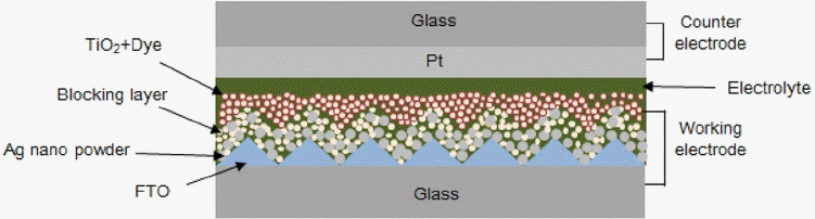
The CE was prepared by RF sputter (MHS-1500, Moohan, 300 W, 13.56 MHz) to form a 100 nm-Pt film on a glass substrate using 99.99% Pt as a target. A flow of 40 sccm Ar at pressure of 5 mtorr at RT was set for the process. The prepared WE and CE were fixed at position and filled with electrolyte, finalizing DSSC device consisted glass/FTO/BL (TiO2 with Ag nano powder)/TiO2/dye (N719)/electrolyte/100 nm Pt/glass with active area of 0.45 cm2 as shown in Fig. 1.
Impedance of DSSC was determined by solar simulator (PEC-L11, Peccell) and potentiostat (Iviumstat, Ivium) to verify interfacial resistance. The analysis was carried out in the frequency range of 10 mHz ~ 1 MHz applying AC voltage and collecting the current responses. I-V (current-voltage) characteristic of DSSC was measured by the same instruments under a setup; a 100 W Xenon lamp was the illumination source at 1 sun (100 mW/cm2) condition. From the I-V curves, short-circuit current density (Jsc), open-circuit voltage (Voc), fill factor (FF), and ECE were evaluated.
3. Results and Discussion
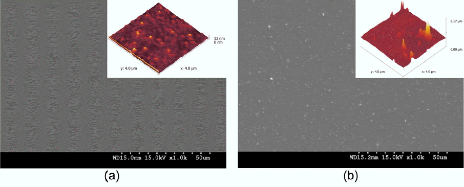
Figure 2 shows FE-SEM surface images of the BL with (a) 0.0 wt% and (b) 0.5 wt% of Ag nano powders, respectively. AFM images shown in the upper right corner. Fig. 2(a) shows uniform coating of the BL without impurities by using spin coating. The RMS value of 1.07 nm was indicated through the AFM result inset at the upper right corner.
Figure 2(b) shows that Ag nano powers with a particle size of an average of 200 nm could be actually confirmed having a particle size of less than about 150 nm due to agglomeration of Ag in the coating process. Also, as shown in the inset, an average RMS value of 7.90 nm was observed. The increase in specific surface areas was confirmed to be possible as a result of addition of Ag nano powder, which was expected to be indirectly advantageous to an increase in specific reaction areas of the upper TiO2 layer.
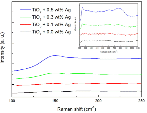
Figure 3 shows micro-Raman results of the BL with 0.0 ~ 0.5 wt% of Ag nano powders. In the case of BL, it is composed of TiO2, and the Raman characteristic peaks of TiO2 appear at 144, 199, 399, 516, and 640 cm−1.16) The graph in the upper right corner represents the results where the BLs with dispersion of 0.0 ~ 0.5 wt% of Ag nano powder were confirmed in the Raman shift range of 100 ~ 1100 cm−1 and other peaks were not observed although a Raman characteristic peak for TiO2 could be confirmed at 144 cm−1. This suggests that there was a difficulty in measurement because of a very small thickness of 300 nm in the case of BL.
Meanwhile, in the case of confirmation in the Raman shift range of 100 ~ 250 cm−1 to clearly confirm that the intensity of Raman characteristic peak at 144 cm−1 was gradually increased as a result of an increase in added amounts of Ag nano powder. This is the result of an increase in the absolute amounts of incident light was increased due to LSPR phenomenon which the incident light vibrates through resonating interaction with free electrons of Ag nano powder. Such result was in agreement with the report by J. Xu et al.16) where the intensity of Raman characteristic peaks was increased by addition of Ag nano particles to TiO2 layer.
Therefore, occurrence of LSPR phenomenon upon addition of Ag nano powder to the BL has been hereby confirmed.
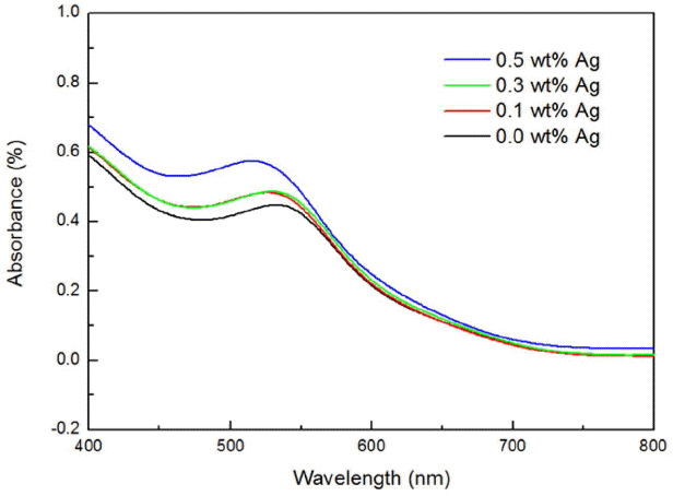
Figure 4 shows the result of measuring absorption in the visible light domain of 400 ~ 800 nm range for the WE having a structure of glass/BL (TiO2 with Ag nano powder)/TiO2/N719 with addition of 0.0 ~ 0.5 wt% of Ag nano powder.
An average absorption of the WE with addition of 0.0 wt% of Ag nano powder was shown to be 0.2433%, and 0.2566%, 0.2616%, and 0.3002% in the case of 0.1 wt%, 0.3 wt%, 0.5 wt%, respectively, confirming that the absorption was increased by addition of Ag nano powder. This was considered to be the result caused by an increase in absorption due to LSPR effects as in the previous micro-Raman result by addition of nano-class Ag powder. Thus, an increase in the absorption was confirmed through LSPR phenomenon as a result of addition of Ag nano powder to the BL.
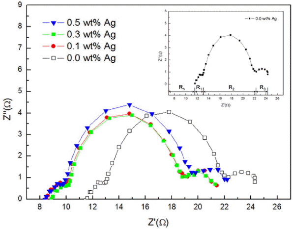
Figure 5 shows the Nyquist diagram consisting of real number and imaginary number for the frequency applied to the DSSC device having a structure of glass/FTO/BL (TiO2 with Ag nano powder)/TiO2/dye (N719)/electrolyte/100 nm Pt/glass with addition of 0.0 ~ 0.5 wt% of Ag nano powder. Parts of each resistance Rh, R1, R2, R3 are also displayed in the Nyquist diagram graph for the device with addition of 0.0 wt% of Ag in the upper right corner.
Rh value is a factor for showing the sheet resistance and the resistance of TCO/electrolyte interface, and Rh values were shown to be 11.60 Ω, 8.48 Ω, 8.86 Ω, and 8.50 Ω upon addition of 0.0, 0.1, 0.3, 0.5 wt% of Ag nano powder, respectively, confirming reduction as a result of addition of Ag nano powder. This was considered to be the result caused by reduction in overall sheet resistance upon employment of Ag having a resistivity of 1.62 × 10⁻⁶ Ω·cm.
R1 value represents an interface resistance related to the resistance of TCO/TiO2 and interface and the resistance to movement of electric charges at TiO2/electrolyte interface, and was shown to be about 1.2 Ω identically for all devices with addition of 0.0 ~ 0.5 wt% of Ag nano powder. This was considered as the result produced by use of the same Pt CE and electrolyte.
R2 value represents a factor showing the resistance to electron movement in TiO2 and the TiO2/electrolyte interface resistance at 1-103 Hz, and is shown to be 9.40 Ω, 9.45 Ω, 8.83 Ω, and 10.06 Ω upon addition of 0.0, 0.1, 0.3, and 0.5 wt% of Ag nano powder, respectively. In particular, a decrease in R2 values can be confirmed up to 0.3 wt%, which was considered to be the result of an increase in electron generation due to LSPR effects as in the previous result of absorption. An increase in R2 values can also be confirmed upon addition of the amounts more than 0.3 wt%, which was considered to be the result caused by relative reduction in fractions of TiO2 playing a role as an electron transport path.
Meanwhile, R3 value corresponds to the Warburg impedance related to diffusion of oxidation-reduction species in the electrolyte at higher frequencies than 106 Hz, and was measured to be about 2.2 Ω in all cases within the range of error, which was considered to be the result produced by use of the same electrolyte.
Thus, we confirmed that the addition of proper Ag nano powders into the BL increased in generating electrons by LSPR effects, which reduced resistance compared to the case of bare blocking layer.
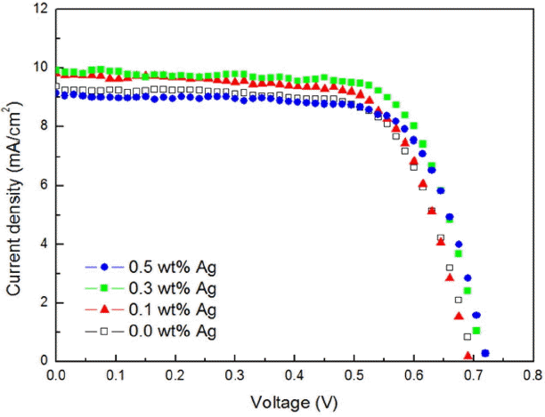
Figure 6 shows I-V data for the DSSC device having a structure of glass/FTO/BL (TiO2 with Ag nano powder)/TiO2/dye (N719)/electrolyte/100 nm Pt/glass with addition of 0.0 ~ 0.5 wt% of Ag nano powder.
In the case of a device having no addition of Ag nano powder, the FF could be confirmed to be smaller as compared with a device having addition of Ag nano powder, and confirmed to be increased with an increase in added amounts of Ag nano powder. Voc were observed within the error range, while the Jsc could be confirmed to be reduced upon addition of more than 0.3 wt% after an increase up to 0.3 wt%.
Table 1 is a summary of results for I-V curves of Fig. 6. Voc were 0.70, 0.69, 0.72, and 0.72 V with 0.0, 0.1, 0.3, and 0.5 wt% of Ag nano powder, respectively. It showed similar values within the error range. Voc were considered attributable to the use of the same electrolyte in all of the present experiments as an element related to oxidation-reduction reaction of the electrolyte.
Jsc was 9.29 mA/cm2 in the device with addition of 0.0 wt% of Ag nano powder, while the values of 9.71 mA/cm2 and 9.98 mA/cm2 were observed in the case of 0.1 wt% and 0.3 wt%, respectively. Jsc was increased with an increase in added amounts of Ag nano powder. This was the result from LSPR effects with addition of Ag nano powder, and was in agreement with the previous impedance result. Meanwhile, reduction in the Jsc to 9.08 mA/cm2 in the case of 0.5 wt% was due to relative reduction in fractions of TiO2 playing a role of electron movement path upon lots of Ag nano powders as in the previous impedance result.
In the case of FF, the value of 0.665 was observed in the device with addition of 0.0 wt% Ag nano powder. Otherwise, 0.673, 0.679, and 0.683 were confirmed in the case of 0.1, 0.3, and 0.5 wt%, respectively. This result was due to increasing a specific surface area.
ECE of device without Ag nano powder was 4.31%, while ECE of device with 0.3 wt% Ag nano powders was 4.80%. This was the result from increasing Jsc and FF according to LSPR effects.
In summary, we successfully fabricated DSSC devices of enhanced ECE with LSPR effects by adding a proper amount of Ag nano powders into the BL.
4. Conclusions
We employed 0.0 ~ 0.5 wt% of Ag nano powders into the BLs of DSSCs, and characterized their properties. Microstructure analysis revealed that Ag nano powders with a particle size of less than 150 nm were successfully dispersed in the BLs. The intensities of Raman characteristic peaks for TiO2 were confirmed to be increased due to LSPR effects with the amount of added Ag nano powders. The absorbance increased with the amounts of added Ag nano powders. The ECEs of DSSC devices improved with the addition of Ag nano powders due to LSPR effects. Thus, by employing the appropriate amount of Ag nano powers, we demonstrated an improvement on ECE of DSSC.