


1. Introduction
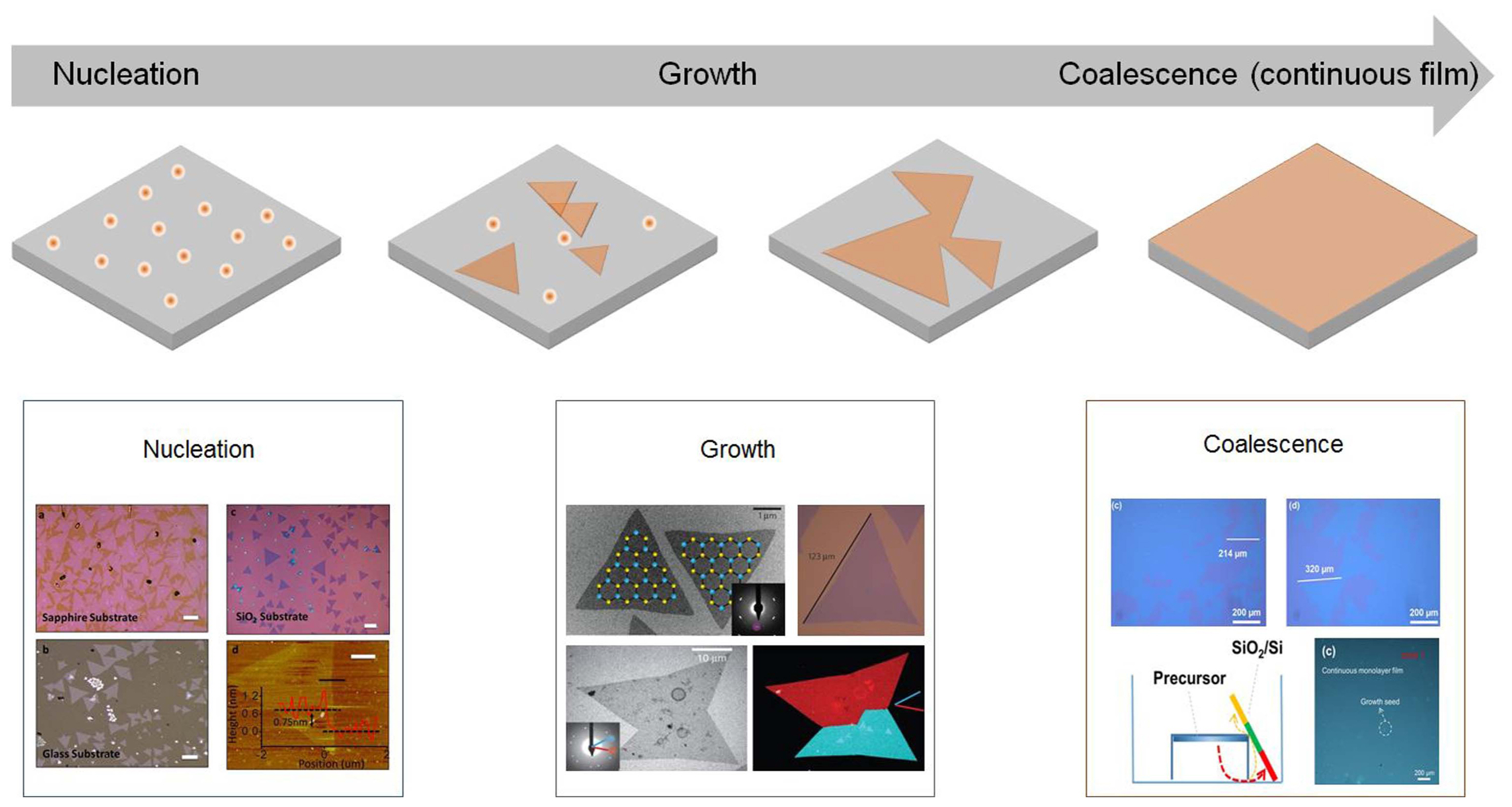
Two-dimensional transition metal dichalcogenides (TMDCs) are a class of ultrathin semiconductors, which could serve as building blocks for next-generation technology. Atomically thin layers of these materials have been fabricated through simple mechanical exfoliation using a Scotch tape. This technique can produce crystalline and defect-free TMDC layers with excellent electronic properties; however, it is not scalable for industrial production. Therefore, many researchers have focused on the large-scale growth of 2D TMDCs using alternative techniques, such as chemical vapor deposition (CVD). CVD enables the growth of TMDCs in large-scale; however, issues related to the crystalline quality of the samples remain. Several contingencies, such as defects, grain boundaries (GBs), and wrinkles, can affect the TMDC properties.1) Recently, many studies have been undertaken to control the many variables at play in CVD and optimize the quality of 2D TMDCs. The optimization strategies focused on different stages of the CVD process, such as nucleation, growth, and coalescence (formation of a continuous film), as shown in Fig. 1. For example, considering that the nucleation density determines the final film quality, the CVD parameters can be tuned to obtain a low number of nuclei that will ultimately merge into a continuous film made of a few single-crystal domains.2) In general, control on the nucleation enables significant improvements in the surface coverage, layer thickness, and crystallinity. Other studies have focused on the GBs between adjacent TMDC grains,3) because the presence of GBs in a polycrystalline film can significantly affect its electrical property. Control of GBs plays an important role also in view of industrial production, where material properties have to be predetermined and fully reproducible.4)
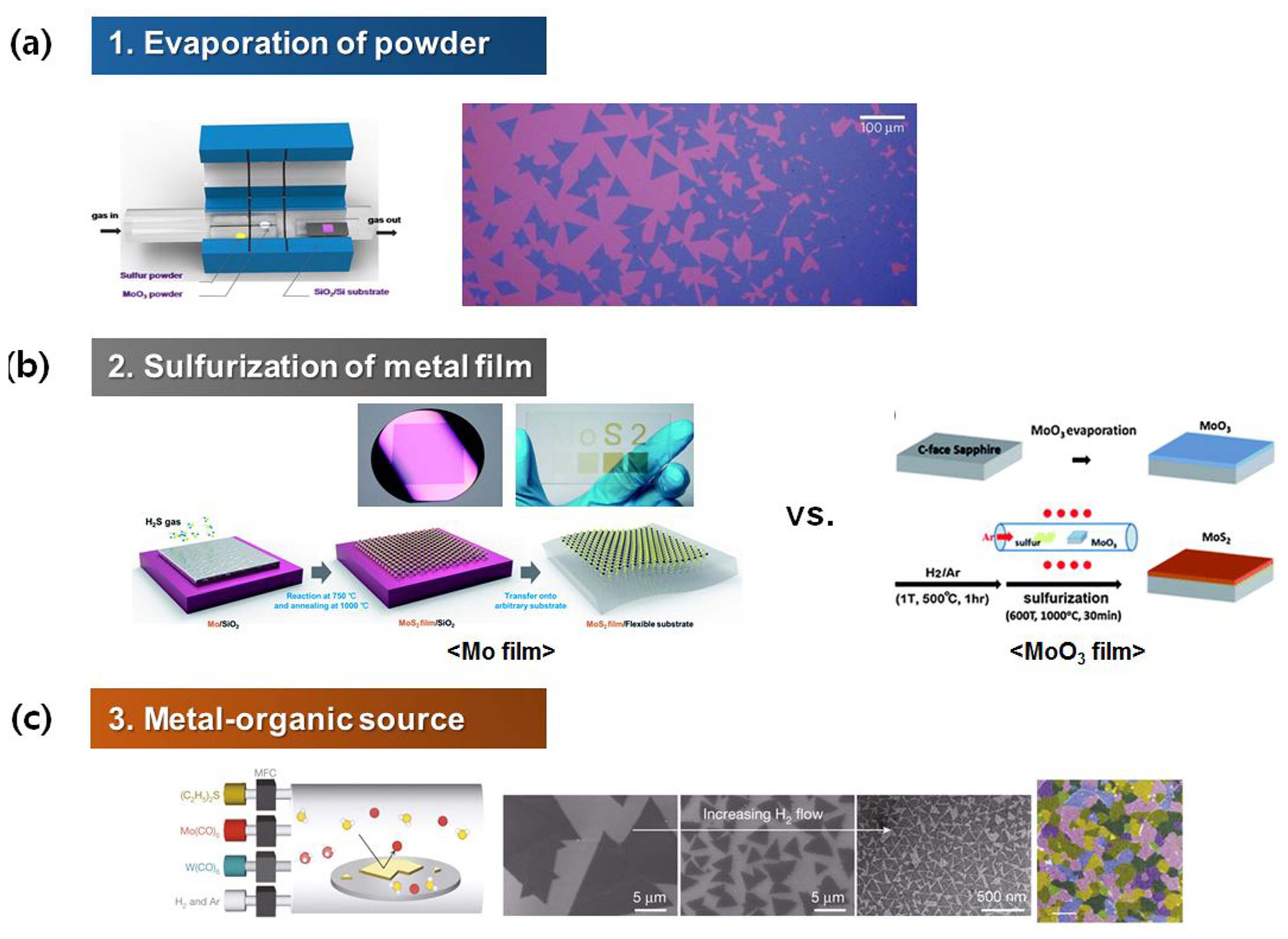
CVD is a promising technique for the growth of large-scale high-quality TMDC thin films. Various approaches have been used to deposit 2D TMDC on different kinds of substrates: (i) The evaporation of precursors in powder form is an effective means to supply the gas phase for growth (Fig. 2(a)). Usually, three different temperature zones are available to separately evaporate the metal source (such as MoO3 and WO3) and chalcogen source (such as S and Se) while the substrate is maintained at a different temperature.3,5) For example, MoO3 vapor is decomposed to Mo to react with sulfur vapor, leading to the formation of MoS2 nuclei, which progressively expand into atomically thin crystals. (ii) Another approach is based on the reaction between a pre-deposited Mo or MoO3 thin film and sulfur precursor gas (Fig. 2(b)).6,7) The Mo or MoO3 thin film with a thickness of a few tens of nanometers is deposited on the substrate by ebeam or thermal evaporation. The Mo surface usually becomes oxidized under ambient conditions during growth. This oxidized surface can be reduced by hydrogen gas. The MoO3 layer is, therefore, reduced to MoO2 or other reduced forms. After pre-annealing, prompt annealing at 1000°C in a sulfur gas atmosphere leads to the formation of a crystalline MoS2 thin film. (iii) In metal-organic chemical vapor deposition (MOCVD), metal-organic gas precursors, such as Mo(CO)6, W(CO)6, and (C2H5)2S, are pyrolyzed on the target substrate for the growth of single-crystal or polycrystalline 2D TMDCs. Even though large-scale growth is possible at low temperatures, the required growth time might be over 12 h, which is significantly longer than in the other approaches. Fig. 2(c) shows a sketch of the MOCVD growth process and optical images of 2D MoS2 grown on a Si/SiO2 substrate.8) Because the gas phase precursors are generally diluted in a mixture of Ar and H2 carrier gases and the partial pressure of each reactant has to be precisely controlled throughout the process for large-scale growth, optimization of the process conditions in MOCVD is trickier.
2. Nucleation
2.1. Homogeneous nucleation growth
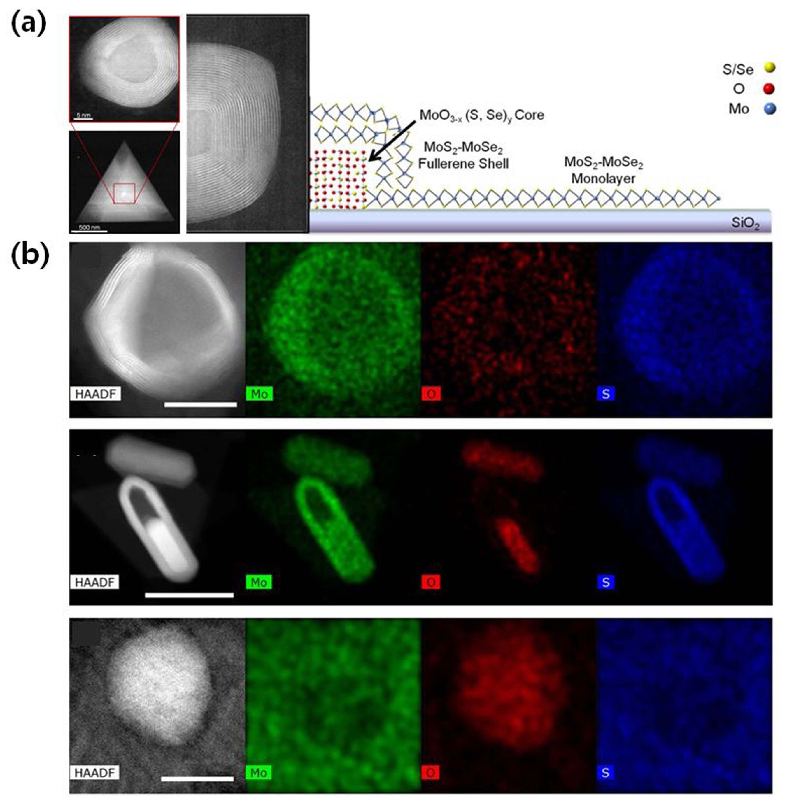
CVD is a widely employed technique that can be used to grow 2D TMDCs for various semiconductor applications. Among the various studies on the CVD of TMDCs, only a few researchers have focused on the details of the nucleation and growth mechanisms. Understanding these mechanisms will help scaling up the growth and facilitate an industrial production. Recently, Cain et al.9) elucidated the various stages of nucleation and growth of TMDCs. They directly grew single- and few-layer MoS2 and MoSe2 samples on ultrathin amorphous SiO2 membranes, as shown in Fig. 3(a). In their work, a partially sulfurized/selenized molybdenum trioxide (MoO3−x(S,Se)y) core was fully covered with a fullerene-like shell of MoS2-MoSe2, as confirmed by aberration-corrected scanning transmission electron microscopy (STEM) imaging and energy-dispersive spectroscopy (EDS) mapping. As shown in Fig. 3(b), Zhu et al.10) carried out a transmission electron microscopy (TEM) study to reveal MoS2 growth kinetics when aided by nucleation seeds. They investigated the morphology, edge structure, and edge terminations at the atomic scale. The direct growth of few-layer and monolayer MoS2 onto graphene-based TEM grids aided direct TEM characterization without any transfer processes. Understanding these mechanisms can provide useful information to control the nucleation and growth of 2D TMDC materials.
2.2. Heterogeneous nucleation growth
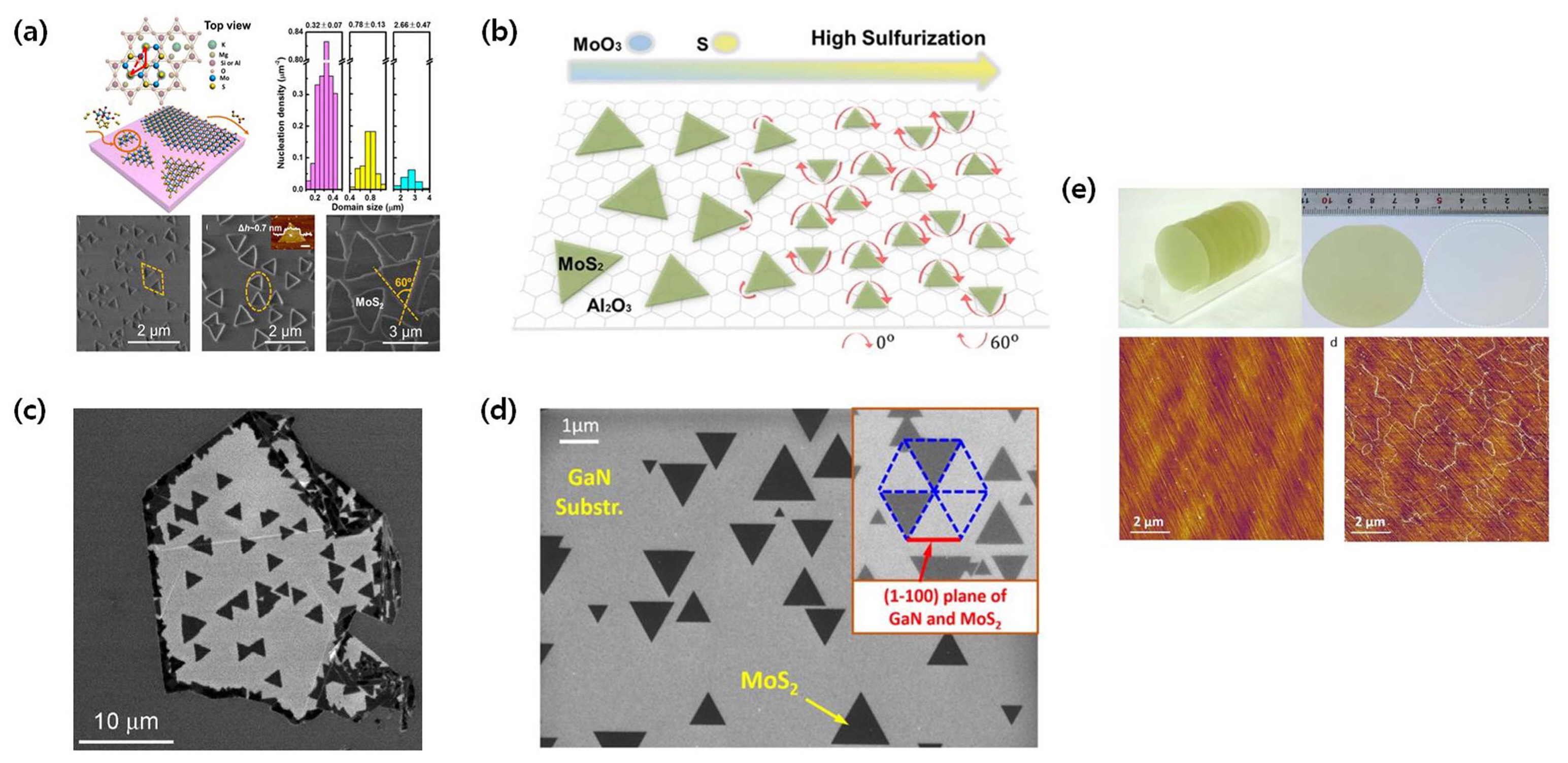
TMDCs are a class of materials with potential in various semiconductor applications. Many scientists have devoted their efforts to devise a production technique for monolayer TMDC, which would grant high yield and precise control on its properties, and ideally not require high-temperature processes (< 650°C). Although the conventional fabrication techniques still present several issues and hamper large-scale TMDCs, some progress has been made in lowering the required process temperatures using ammonium heptamolybdate (AHM),11) reduced graphene oxide,12) or patterned PT/Ti dots13) as seeding promoters on the SiO2/Si substrate. Conventionally, MoS2 island layers can be grown on various substrates without seeds;12) however, the presence of seeding materials can favor the formation of initial nucleation sites that will foster the lateral growth of MoS2 crystals. Using perylene-3,4,9,10-tetracarboxylic acid tetrapotassium salt (PTAS) as a seeding promoter material, Ling et al.14) synthesized monolayer MoS2 at a low process temperature (~ 650°C), as shown in Fig. 4(a). Various aromatic molecules can also be used as effective seeding promoters to reduce the process temperature and increase the yield. The aromatic structure of these molecules is strongly related to the sublimation and decomposition temperatures. Table 1 reports the process conditions and properties of MoS2 films grown with different seeding promoters. Seeding promoters are an effective means to control growth; however, the position of the grown MoS2 crystal cannot be controlled and still remains random. Precise control of the crystal’s position on the substrate is vital for the industry. Li et al.15) used prepatterned metal (e.g., Au) nanoparticles as seeding materials to induce the formation of patterned geometries of monolayer MoS2 through CVD (Fig. 4(b)). In their work, MoS2 growth was lateral rather than vertical because of the more favorable thermodynamic driving force along the in-plane direction.16) Studies of this kind can advance the design of patterned TMDC growth for future electronic industry.
3. Control of Shape and Edge
Unlike graphene, TMDCs are composed of two different elements; therefore, they have to be synthesized with two or more kinds of precursors. This adds to the complexity of the process, which might lower reproducibility. To solve this problem, several researchers studied in detail the effect of the concentration of precursors during TMDC growth. Using powder precursors, Wang et al.17) experimentally (in Fig. 5(a)) demonstrated that the ratio of Mo and S affects the resultant shape and edge structure of MoS2 crystals, as shown in Fig. 5(b). When the ratio changes and the amount of molybdenum increases, triangular grains with only Mo-zz termination edge form. Conversely, when the sulfur ratio increases, triangular grains with only S-zz termination edge form. To explain this, Rajan et al.18) performed theoretical calculations on the effect of the concentration ratio of two precursors, as shown in Fig. 5c. In their work, the optimal precursor concentrations were calculated to devise a systematic growth method with high reproducibility. Through proper control of the precursor ratio, a desired shape and edge structure was achieved, and hence the resulting effect on the TMDC properties was revealed. As shown in Fig. 5(d), Cao et al.19) computationally analyzed the shape and edge structure of MoS2 single grains, and revealed magnetism characteristics. These series of calculations demonstrate the possibility of various catalytic activities as well as the synthesis of grains with the desired electronic and magnetic states by controlling the chemical potential through edge state control.20)
4. Kinetics and Thermodynamics in Growth
As shown in Fig. 6(a), the basic principle for thin-film growth is that the process proceeds in the most thermodynamically stable state. In this respect, it is very difficult to analyze the growth process in situ, because the process usually takes place in a sealed environment and at a high temperature. In addition, since the growth occurs in stages, it is too complicated to predict its evolution across the stages. In general, a kinetic and thermodynamic analysis of the process is the most advisable route to analyze and control the growth reaction. As shown in Fig. 6(b) and (c), Shang et al.16) proposed an analytical interpretation of the lateral and vertical growth of TMDCs by calculating the Gibbs free energy and investigating the phase diagrams of the various reactions occurring during MoS2 growth. Ye et al.21) analyzed both the in-plane growth of a layer and the formation of vertically stacked layers in relation to the temperature and precursor mass flow rate, as shown in Fig. 6(d) and (e). Their results suggest the possibility of qualitative and quantitative theoretical calculations that can estimate expected experimental results, thereby providing guidance for the design of effective growth processes.
5. Epitaxial Growth
As routinely used in the Si semiconductor industry, the epitaxial growth of TMDCs on single-crystal substrates is a viable approach. Several researchers have successfully grown different 2D TMDCs onto highly crystalline substrates, such as c-sapphire,22,23) mica24) (Fig. 7(a)), GaN25) (Fig. 7(d)), h-BN26) (Fig. 7(c)), SrTiO3,27) and MoS2,28) where the grain orientation and crystallization can be finely controlled. Aljarb et al.22) used annealed c-sapphire substrates for seed-assisted growth, and grew large-scale single-crystal MoS2 films. In their experiments, a highly sulfurized environment was shown to allow the efficient and aligned growth of MoS2 single crystals at a moderate temperature (800°C), as shown in Fig. 7(b). Chen et al.28) also performed highly organized homo-epitaxial growth using monolayer MoS2 as a substrate. Recently, Yu et al.23) succeeded in synthesizing highly oriented wafer-scale MoS2 using a sapphire substrate. The synthesized MoS2 had a highly ordered orientation distribution (~ 3° difference) (Fig. 7(e)). This highly oriented MoS2 film could be easily peeled off from the sapphire substrate by simply immersing the substrate into water. In addition, Zhang et al.29) used MOCVD to grow WSe2 grains aligned to the 0° or 60° directions of the sapphire substrate. These results show that growth on a substrate is key toward the growth of large-area, high-quality TMDCs.
6. Assisted Growth
Difficulties in optimizing the multi-factor CVD process for the growth of TMDCs have driven researchers to explore alternative approaches for the growth of high-quality TMDCs. In particular, promoters capable of inducing the hetero-nucleation of TMDC crystals have been targeted. Among them, the most popular promoter, PTAS,14) has a molecular structure which enables TMDC growth without affecting the crystal properties. Similarly, as shown in Fig. 8(a), Choi et al. has succeeded in synthesizing high-quality MoS2 which suppresses sub-reaction by using H2O as a weak oxidizer during the MOCVD process.30) Also, many researchers created the hydroxyl form of metal oxide by supplying H2O molecules31-33) for the efficient growth of WS2, which helped overcome the high thermal stability of metal oxide and more efficiently supplied metal atoms in a vapor state, leading to the growth of high-quality TMDCs. The biggest issue in conventional CVD growth using precursors in powder form is the chalcogenization of the metal source powder, which render it difficult to evaporate, causing a deficiency of metal atoms during the growth. As shown in Fig. 8(b), to prevent a shortage of the metal source, Chen et al.34) maintained a uniform supply of the metal source vapor by oxidizing the metal source with a small amount of oxygen gas. Thus, they succeeded in synthesizing MoS2 single crystals with high quality and large sizes. As shown in Fig. 8(c), Zhou et al.35) reported the growth of large, single-crystal MoS2 using an alkali metal halide. In their work, a metal oxychloride sub-reaction material was supplied instead of the conventional metal oxide vapor, resulting in the growth of a high-quality single-crystal MoS2 monolayer. Li et al.36,37) also utilized alkali metal halide to synthesize various high-quality TMDCs. As shown in Fig. 8(d), MoS2 nanoribbons with a width of tens to thousands of nanometers were fabricated through the vapor-liquid-solid (VLS) reaction. The small amount of additives that act as nucleation seeds or growth promoters enables an improvement in the TMDC quality and in the growth control.
7. Growth of Vertical and Lateral Heterostructures
TMDCs have shown unprecedented properties in the monolayer limit. Hence, a combination of many TMDC monolayers, for example, vertical and lateral heterostructures, can provide plenty of room to investigate novel properties at the junction of two (or more) different TMDCs. Even though multilayered heterostructures of TMDCs have been realized by transferring multiple layers, a more convenient and efficient way to fabricate large-scale and clean heterostructures is required. To overcome these drawbacks, many research groups have tried to directly fabricate assembled heterostructures during growth. As shown in Fig. 9, Gong et al.38) succeeded in synthesizing laterally (or vertically) stacked heterostructures by controlling the process temperature in a two-step growth process. At relatively low process temperatures of 650°C, the precursor did not overcome the activation energy required for vertical stacking of the additional layer on the basal plane of the previously grown TMDC layer. Therefore, the precursors bonded to a dangling bond at the edge site with a high surface energy, leading to the formation of an in-plane heterostructure. On the contrary, a high process temperature (850°C) resulted in the growth of a vertically stacked heterostructure. Very recently, it was demonstrated that a Janus structure (in which two planes of different chalcogen atoms make the sandwich structure with the central metallic plane) can be synthesized, as shown in Fig. 10(a).39) To fabricate the Janus plane of MoSSe, an intermediate state of MoSH, where the chalcogen atoms in the top MoS2 layer are substituted with H by hydrogen plasma, is prepared and then the Janus structure is formed by replacing hydrogen atoms with Se. Starting with MoSe2, Zhang et al.40) also showed that the formation of the Janus structure is possible via direct sulfurization of the top surface of previously grown MoSe2, as shown in Fig. 10(b).
8. Vertical and Helical Growth
As shown in Fig. 11(a), Kong et al.41) successfully grew vertically aligned TMDC layers instead of the usually reported planar or nanoflower TMDC structures. Horizontally growing TMDC layers have a limited catalytic effect owing to the absence of dangling bonds on the surface. However, during the growth of vertically aligned TMDCs, edge sites with a high surface energy (owing to dangling bonds) act as highly catalytic sites for the growth reactions. Therefore, the precise elucidation and control of these growth mechanisms is crucial for the growth of vertically aligned TMDCs. Occasionally, helically grown TMDCs were observed as reported by Zhang et al. (Fig. 11(b)).42) Owing to the helical structure, the TMDCs showed optically active characteristics, which are in contrast to the properties of pyramid-shape multilayers. 43)
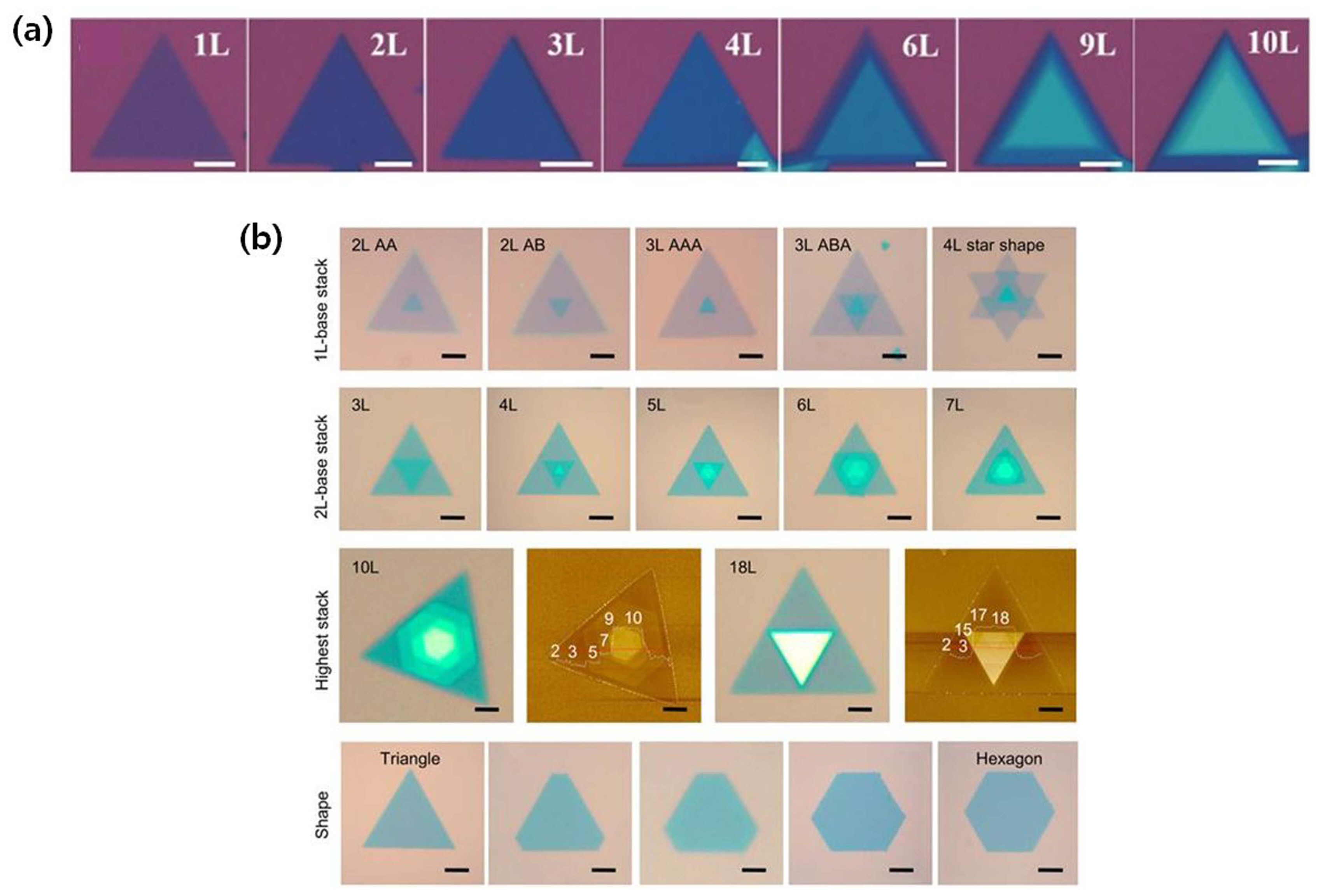
9. Control of Layers and Stacking Order
One of the unique characteristics of the TMDCs is that the band structure and band-gap size can be controlled by adjusting their thickness (i.e., the number of layers). However, there has been no clear way to control the thickness of TMDCs at the atomic layer scale in CVD because the monolayer is thermodynamically favorable. In TMDCs, there are no dangling bonds on the surface of the basal plane; however, dangling bonds are present at edge sites. Owing to the higher energy of edge sites (approximately 100 times higher than that of the basal plane), in-plane growth is particularly favorable.44) Because of such stability of the basal plane, the precursor molecules deposited on the basal plane diffuse to the active edge sites and form thick layers at the edge.45) Therefore, thick TMDC crystals can be grown in the optimized growth condition. When the amount of the metal source is higher than that of the chalcogen source, layer-by-layer growth is more favorable than in-plane growth. As shown in Fig. 12(a), Zheng et al.46) successfully synthesized MoS2 with different thicknesses by CVD and electrochemically oxidized Mo films. High-quality MoS2 triangular single crystals were fabricated from a monolayer to ten layers by controlling the pressure of Mo from the pre-oxidized Mo film. Even in similar multilayers, the stacking order might be different. As shown in Fig. 12(b), Shinde et al.47) synthesized various multilayers with different stacking types of H or R using NaCl as a promoter. Because multilayer TMDCs with different stacking sequences have distinct optical properties owing to the different interlayer coupling, control of the stacking order is critical for optical applications of multilayer TMDCs. Advanced MOCVD is a promising technique for the growth of multilayer TMDCs. However, MOCVD requires a long growth time for thick TMDCs owing to the very small amount of the supplied sources. Therefore, a new growth method, which enables the growth of multilayer TMDCs with controlled stacking order in a short time is needed for practical applications of TMDCs.
10. Phase Control in Growth
A distorted octahedral coordination leads to a metallic electronic structure, forming a 1T′ phase, whereas a trigonal prismatic coordination forms a 2H phase, indicating semi-conducting property. Molybdenum-based TMDCs are generally stable in the 2H phase under ambient conditions. In the monolayer form, the 2H phase of the semiconductor (which has a band gap of 1-2 eV) has no inversion symmetry, thereby leading to the generation of spin-split bands near the K-point of the Brillouin zone. In contrast, both 1T′ and 1T phases are metallic with inversion symmetry. Therefore, the phase transition of Mo-based TMDCs leads to variations in electrical properties, which can be utilized for various electronic applications.48-51) Sung et al.52) synthesized metallic (1T′) and semiconducting (2H) MoTe2 crystals within the same atomic plane by using hetero-epitaxial CVD with high-purity precursors MoO3 and Te and the promoter NaCl. As shown in Fig. 13(a), to selectively stabilize each phase, the supply of NaCl and the process temperature were precisely controlled during the CVD. Empante et al.53) fabricated three different MoTe2 phases, 1T, 1T′, and 2H, by changing the growth quenching temperature (Fig. 13(b)).
11. Outlook
In the beginning stage of TMDC growth, solid precursors in powder form are evaporated to supply precursor molecules. However, when solid precursors are used, it is not possible to maintain constant source concentrations and uniform deposition of the evaporated molecules. This limitation makes it difficult to utilize the current TMDC growth method for industrial purposes. To overcome this issue, modified CVD processes have been proposed. Recently, the control of phases and morphologies in the synthesis of TMDCs has received attention. Despite the discovery of growth mechanisms and their development, there are still many issues regarding the scalability, quality, reproducibility, and degradation. Nevertheless, the recent progress in the growth of TMDCs shows great promise to address existing issues.